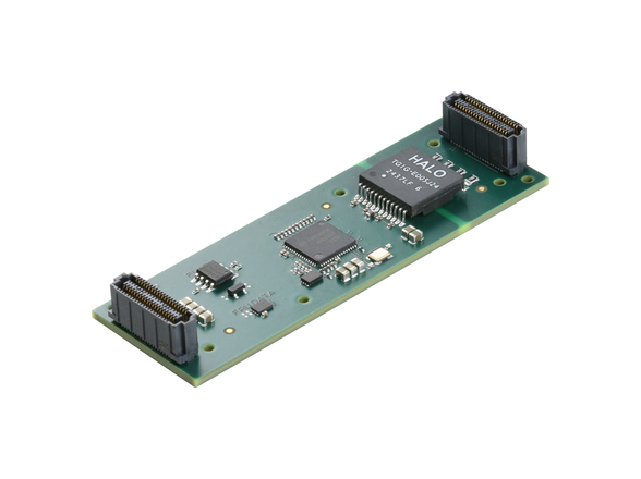
| AD1520 Dual Channel 1.5GSPS 8-bit ADC XMC / PMC module from VMETRO |
VMETRO, a leader in embedded computing solutions based on standards such as VXS, VPX, XMC and FMC that utilize multi-gigabit serial interconnects, today announced an improved analog performance high-speed analog input XMC module with the latest generation Xilinx® Virtex®-5 FPGA. The AD1520 is a dual channel 1.5GSPS ADC XMC/PMC module. The analog input of the AD1520 utilizes a National Semiconductor ADC08D1520 8-bit converter that is directly connected to either a Virtex-5 SX95T, LX110T or LX155T FPGA back-end. This combination of high-speed analog input and high-performance FPGA processing is ideal for demanding real-time applications such as Electronic Warfare (EW), Electronic Counter Measures (ECM), Radar and Telecommunications.
The AD1520 board shows typical performance characteristics of 7.4 ENOB, 61 dBc SFDR and 47 db SNR at 373 MHz. The full power input bandwidth extends to beyond 2GHz. All of these metrics improve upon the AD1500 and across the input spectrum.
The AD1520 has LVPECL trigger input and output connections along with sample clock input and general purpose I/Os on the front panel. This connectivity allows the AD1520 to be operated in a range of modes, including multi-board synchronous sampling. A companion product, the XCLK1 clock generator PMC/XMC card, can be used to generate low skew, minimal jitter clock signals to the ADC boards and coordinate multi-board synchronization.
The hardware configuration of the AD1520 is similar to the AD3000, a single channel 3.0GSPS ADC XMC/PMC module. The FPGA is connected to two 9Mbyte memory banks of high bandwidth QDRII SRAM capable of accepting the incoming data at full speed from the ADC and two 128Mbyte banks of DDR2 SDRAM. Although the use of these memories is defined by the application, they can be used to help maximize the FPGAs DSP processing ability and provide large data buffers. FPGA reconfiguration images are stored in local FLASH memory for power up configuration. Alternatively, a JTAG header is provided for code development under the ChipScopeTM Pro development tool chain.
Off board data links are provided through either PCI-X/PCI via the PMC connectors or high-speed, multi-Gbps Virtex-5 RocketIO™ transceivers using the XMC connectors. There are sixteen full-duplex low-power serial transceivers arranged across two XMC connectors. The combined speed of the data links spanning the XMC connectors are capable of streaming data off the AD1520 at the boards maximum sampling rate when using a protocol such as Aurora. A PCI Express® end-point controller is available within the FPGA supporting up to x8 PCIe operation.
Development for the AD1520 is supported by VMETROs FusionXF development kit. FusionXF includes a Software Development Kit (SDK) and an HDL Development Kit (HDK). The SDK provides host software support for Windows, VxWorks and Linux, including drivers for high-speed DMA access between the XMC and host CPU, FPGA reconfiguration and diagnostics. The HDK contains the FPGA interface definitions and HDL functions to build a fully functional FPGA design. Example software and HDL are provided for using the National Semiconductor ADC08D1520 and the external memory with the Virtex-5 FPGA.
The AD1520 is available in XMC and PMC form factors, for air and conduction-cooled environments.


