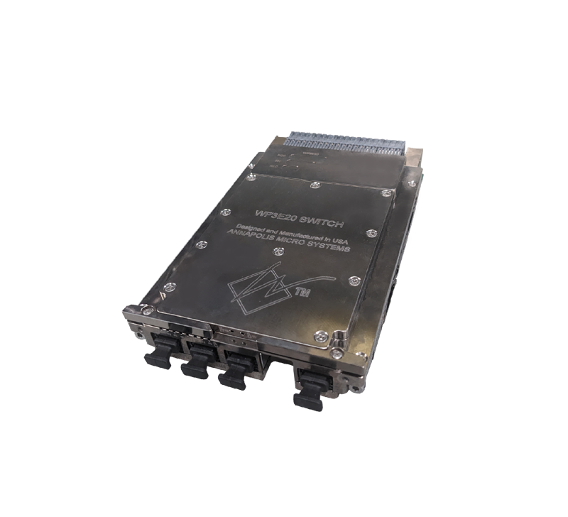
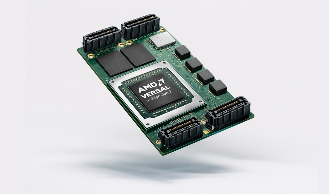
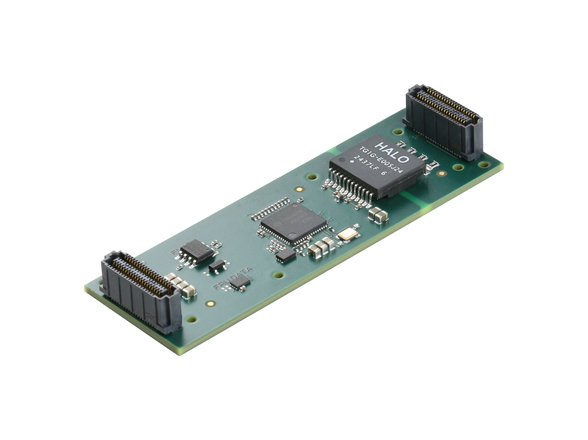
| Figure 1 – VXS Payload Board using QuiXilica V5 Architecture |
Chelmsford, MA – TEK Microsystems, Inc., the leading supplier of VXS-based digitizers has announced its new QuiXilica V5 Architecture designed to meet the needs of demanding sensor-processing applications across a range of environments. The QuiXilica V5 architecture uses the latest field programmable gate array (FPGA) based processors – the Xilinx Virtex®-5 family, advanced DDR3 SDRAM, and the latest communications technologies available. Full ruggedization has been designed into the architecture from the outset to provide products suitable for harsh demanding environments and deployed systems.
“Advanced applications in Radar, EW, ELINT, SIGINT and Telecom have an insatiable demand for increased performance. Sensors continually require more channels, increased processing capabilities, higher memory performance, and greater communications bandwidth. To meet these demands requires the very latest technologies including FPGAs, memories, and communications standards”, comments TEK Microsystems, Inc. president and CTO Andrew Reddig. “To get the best out of the latest component technologies, we have taken a holistic approach to the development of the QuiXilica V5 Architecture. It is a design philosophy that logically follows and meets the data flow requirements of these advanced applications. A complete family of QuiXilica V5 digitizer boards and data recording systems will begin to be available in the next 30 to 60 days.”
The QuiXilica V5 Architecture (shown in Figure 1) uses three Xilinx Virtex-5 FPGAs, DDR3 SDRAM and the latest enhancements in flexible I/O communication modules (SFP+ and QSFP). Firmware and software support for a range of open standards and protocols is provided including Gigabit Ethernet, Serial FPDP (ANSI VITA 17.1 and 17.2) and Fibre Channel. For inter-FPGA and inter-board communications, other protocol support is provided such as Xilinx Aurora and PCI Express. A very broad range of analog sensor I/O configurations provide easy compatibility with the widest range of analog signal options, addressing multi-channel, high resolution sampled data requirements at 4 Gsps (Gigasamples per second) and beyond.
Products will be initially released in a 6U VITA 41.0 (VXS) format with other form factors to follow later in 2008.
QuiXilica V5 Architecture Overview
The QuiXilica V5 Architecture is the basis for a variety of digitizer boards in multiple form factors. Initial members of the QuiXilica V5 Family use three Xilinx Virtex-5 FPGAs to provide maximum high bandwidth processing and system configuration flexibility. Each FPGA has access to two banks of DDR3 SDRAM of 512 MB each (1 GB total per FPGA). The QuiXilica V5 Architecture products will support 2 GB and 4 GB per FPGA when larger memory devices are available for increased storage density and increased memory bandwidth. Memory and FPGAs have been combined and interconnected using multiple high bandwidth parallel and high-speed serial interconnections; thus data can be available within the processing chain as needed to meet a wide range of application requirements.
Inter-board and system communication requirements are met using either backplane connections or multiple front-panel high speed serial Quad Small Form-Factor Pluggable (QSFP) and Small Form-Factor Pluggable (SFP+) modules which provide eight and six high speed serial links respectively operating at up to 6.5 Gb/s. Utilizing the embedded communication functions as well as Tekmicros QuiXilica core and software library support (QuiXtream), the QuiXilica V5 Family supports the latest generation of Open Standard I/O protocols such as Gigabit Ethernet, Serial FPDP (ANSI VITA 17.1 & 17.2), PCI Express, Xilinx Aurora and Fibre Channel.
In addition to providing high performance, QuiXilica V5 digitizers have been designed for ruggedization and power management. The DDR3 SDRAM uses 17% less power than DDR2. QuiXilica V5 boards operate effectively in laboratory, rugged air-cooled, and rugged conduction-cooled environments to meet the needs of deployed applications.
TEK Microsystems provides superior QuiXilica FPGA cores and supporting firmware to minimize the effort required to extract maximum performance from the architecture, and to make development as easy as possible.
The Architectures common hardware interfaces and firmware /software development tools allow the user to easily migrate between platforms as different systems are developed, protecting the users investment both in their FPGA application and in integration and qualification of the QuiXilica V5 products in the target application.
The QuiXilica V5 Architecture provides a simple flexible parallel interface that enables boards to be factory configured with different ADCs and DACs, thus enabling the boards to meet a robust variety of applications. High bandwidth support for ADCs and DACs operating beyond 4 Gsps is designed into the architecture.
Building upon the success of the current QuiXilica board family and retaining a migration path for current users, the analog configuration options that are planned to be available for QuiXilicaV5 digitizers are:
– 6 x 16 bit 160MSPS ADC & 1 x DAC channel
– 7 x 16 bit 500 MHz DAC channels
– 2 x 10 bit 2.2 GHz ADC channels
– 2x 12 bit 2.2 GHz DAC channels
– 1x 10 bit 2.2 GHz ADC channels with 1x 12 bit 2.2 GHz DAC channels
– 6 x 12 bit 500MHz ADC channels
– 2 x 8 bit 4GHz ADCs channels
– + further configurations to be determined
The complexities of FPGA development presents some tough challenges in terms of system monitoring, managing the power supply and heat dissipation. Tekmicro provides software tools to allow users to analyze and experiment with the requirements of their design and the associated impact on power supply requirements. A comprehensive System Health Monitoring facility continuously tracks temperature and supplies current at a number of key points in the system.
Summary
The scalable, configurable QuiXilica V5 Architecture has been designed using the latest FPGA based processing, memory, and communications technologies available. Full ruggedization has been designed into the architecture from the outset, offering availability of products for use in harsh demanding environments for deployed systems.
Firmware and application support is provided to enable users to easily tailor the board to meet their specific design requirements.
QuiXilica V5 has been developed to meet the requirements of data-flow sensor I/O applications making QuiXilica V5 VXS boards the ideal solution for the latest generation of front-end sensor processor development.
TEK Microsystems has prepared a complete white paper on the features and advantages of the QuiXilica V5 Architecture. Please see www.tekmicro.com/PDFs/QuiXilicaV5wp.041508.pdf to download.
For more information, contact Dianne McDermott, 978 394 5166 or [email protected]
About TEK Microsystems, Inc.
Founded in 1981 and headquartered in Chelmsford, Massachusetts, TEK Microsystems, Inc., designs, manufactures and markets a wide range of advanced high-performance boards and systems for embedded real-time data acquisition, data conversion, storage and recording. The Company provides both commercial and rugged grade products which are used in real-time systems designed for applications such as reconnaissance, electronic warfare, signals intelligence, mine detection, medical imaging, radar, sonar, semiconductor inspection and seismic research. For additional information see www.tekmicro.com.


