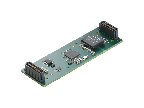
Pentek, Inc., a pioneer in VME board-level technology, today released its Model 7141 Dual Multiband Transceiver with FPGA. It is a complete software radio system for connection to HF or IF ports of a communications system and joins Pentek’s family of high-performance PMC/XMC transceiver modules. The Model 7141 is an enhanced successor to Pentek’s popular Model 7140 transceiver, which is widely deployed by many customers for SIGINT, software radio and communications applications. Pentek has significantly boosted analog performance in the Model 7141 so that the signal-to-noise ratio and the spurious free dynamic range are improved by 10 dB, when compared to many competitive products.
Optimized Signal Quality
“Because our customers typically use signals covering a wide dynamic range, better signal quality means that small signals previously lost in noise can now be detected. This is increasingly important for signal intelligence applications, in particular,” said Rodger Hosking, vice president. “We accomplished our mission for gaining superior analog performance by using proprietary design techniques in the analog front end which was tailored to bring out the best characteristics of the Linear Technology 14-bit A/D converters.”
Hosking went on to explain that even though A/D converter device manufacturers cite attractive specifications, the challenge in realizing these specifications depends primarily on the printed circuit board layout, component shielding and power supply filtering. The Model 7141 actually went through several successive board layouts until Pentek design engineers were satisfied that they had achieved the desired A/D performance––improved signal-to-noise ratio and spurious-free dynamic range.
“Sampling signals in the analog world requires an intimate knowledge of the A/D front end and careful board layout to maximize the full capabilities of the analog to digital converter,” said Alison Steer, Product Marketing manager for Linear Technologys High Speed Data Converter product line. “Pentek’s performance specifications prove they have harnessed the full potential of our high performance LTC2255 A/D to provide the superior combination of speed, quality and optimization. Linear Technology is committed to providing high-performance data converter products for the Software Defined Radio and similar data acquisition applications.”
A/D Converter Stage
The Model 7141 accepts two full scale analog HF or IF inputs on front-panel MMCX connectors at +10 dBm into 50 ohms with transformer coupling into Linear Technologys LTC2255 14-bit 125 MHz A/D converters. A/D output samples are delivered into the Virtex-II Pro FPGA for signal processing or for routing to other module resources.
Digital Downconverter Stage
A TI/Graychip GC4016 quad digital downconverter accepts either four 14-bit inputs or three 16-bit digital inputs from the FPGA, which determines the source of GC4016 input data. These sources include the A/D converters, FPGA signal processing engines, SDRAM delay memory and data sources on the PCI bus. Each GC4016 channel may be set for independent tuning frequency and bandwidth. For an A/D sample clock frequency of 100 MHz, the output bandwidth for each channel ranges from 5 kHz up to 2.5 MHz. By combining two or four channels, output bandwidth of up to 5 or 10 MHz can be achieved.
Digital Upconverter Stage
A TI DAC5686 digital upconverter (DUC) and dual D/A accepts baseband real or complex data streams from the FPGA with signal bandwidths up to 40 MHz. When operating as an upconverter, it interpolates and translates real or complex baseband input signals to any IF center frequency between DC and 160 MHz. It delivers real or quadrature (I+Q) analog outputs through two 320 MHz, 16-bit D/A converters to two front-panel MMCX connectors at +4 dBm into 50 ohms.
If translation is disabled, the DAC5686 acts as a two channel interpolating 16-bit D/A with output sampling rates up to 500 MHz. The optional factory-installed interpolation filter core 450 increases the sampling rate of real or complex baseband signals by a factor of 16 to 2048, programmable in steps of 4, and relieves the host processor from performing upsampling tasks. The interpolation filter can be used in series with the DUCs built-in interpolation, creating an overall interpolation range for the module from x2 to x32,768.
Virtex-II Pro FPGA
The Xilinx XC2VP50 Virtex-II Pro FPGA serves as a control and status engine with data and programming interfaces to each of the on-board resources including the A/D converters, GC4016 digital downconverter, digital upconverter and D/A converters. Factory
Installed FPGA functions include data multiplexing, channel selection, data packing, gating, triggering and SDRAM memory control. The FPGA includes two PowerPC cores that can be used as local microcontrollers to create complete application engines.
Clocking and Synchronization
Two independent internal timing buses can provide either a single clock or two different clock rates for the input and output signals. Each Model 7141 can act as either a timing bus slave receiving timing signals or as a master driving up to seven boards supporting synchronous sampling and sync functions across all connected boards. Up to 80 boards may be synchronized with a Model 9190 Clock and Sync Generator.
2.5 GB/sec XMC Interconnects
The Model 7141s optional XMC connection complies with the VITA 42 XMC specification and supports high-speed switched-fabric interconnects such as Serial RapidIO and PCI Express. Dual 4X links between the XMC module and the carrier board handle serial-bit rates up to 3.125 GHz. These links operate independently of the PCI interface and achieve streaming data transfer rates of up to 2.5 GB/sec.
Software Support and FPGA Development Tools
The Model 7141 is fully supported by Pentek’s ReadyFlow Board Support Packages (BSP). Pentek’s ReadyFlow BSPs simplify board operation and setup with easy-to-use function calls. ReadyFlow libraries offer flexibility and provide low-level access to all of the board’s hardware. Pentek ReadyFlow BSPs and software development tools, plus third-party offerings are all available for a variety of operating systems including Windows 2000/XP, Linux and VxWorks platforms.
The Model 7141 benefits from Pentek’s numerous GateFlow FPGA resources. The GateFlow FPGA Design Kit provides designers with all VHSIC Hardware Description Language (VHDL) source code and device configuration for the basic factory-installed functions to facilitate the addition of custom algorithms. The developer may add proprietary IP to the core that is shipped with Model 7141 to extend functionality of the board. Also available are Pentek’s GateFlow installed IP cores, including wideband and multi-channel digital receivers.
Pricing and Availability
The PMC/XMC commercial version of the Model 7141 Dual Multiband Transceiver with FPGA is priced at $10,995 USD, with delivery 8 to10 weeks ARO. The Model 7141 is also available in PCI or 3U and 6U cPCI form factors and ruggedized versions.

