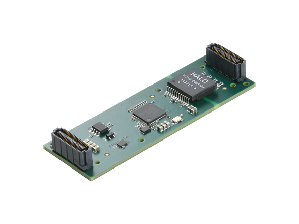
A new mezzanine card standard called FMC+, an important development for embedded computing designs using FPGAs and high-speed I/O, will extend the total number of gigabit transceivers (GTs) in a card from 10 to 32 and increase the maximum data rate from 10 Gbps to 28 Gbps while maintaining backward compatibility with the current FMC standard.
These capabilities mesh nicely with new devices such as those using the JESD204B serial interface standard, as well as 10G and 40G fiber optics and high-speed serial memory. FMC+ addresses the most challenging I/O requirements, offering developers the best of two worlds: the flexibility of a mezzanine card with the I/O density of a monolithic design.
The mezzanine card advantage
Mezzanine cards are an effective and widely used way to add specialized functions to an embedded system. Because they attach to a base or carrier card, rather than plugging directly into a backplane, mezzanine cards can be easily changed. For system designers, this means both configuration flexibility and an easier path to technology upgrades. However, this flexibility usually comes at the cost of functionality due to either connectivity issues or the extra real estate needed to fit on the board.
For FPGAs, the primary open standard is ANSI/VITA 57.1, otherwise known as the FPGA Mezzanine Card (FMC) standard. A new version dubbed FMC+ (or, more formally, VITA 57.4) extends the capabilities of the current FMC standard with a major enhancement to gigabit serial interface functionality.
FMC+ addresses many of the drawbacks of mezzanine-based I/O compared to monolithic solutions, simultaneously delivering both flexibility and performance. At the same time, the FMC+ standard stays true to the FMC history and its installed base by supporting backward compatibility.
The FMC standard defines a small-format mezzanine card, similar in width and height to the long-established XMCs or PMCs, but about half the length. This means FMCs have less component real estate than open-standard formats. However, FMCs do not need bus interfaces such as PCI-X, which often take up a considerable amount of board real estate. Instead, FMCs have direct I/O to the host FPGA, with simplified power supply requirements. This means that despite their size, FMCs could have more I/O capacity than their XMC counterparts. As with the PMC and XMC specifications, FMC and FMC+ define options for both air and conduction cooling, thereby serving both benign and rugged applications in commercial and defense markets.
The anatomy of the FMC specification is simple. The standard allows for up to 160 single-ended or 80 differential parallel I/O signals for high-pin-count (HPC) designs or half that number for low-pin-count (LPC) variants. Up to 10 full-duplex GT connections are specified. The GTs are useful for fiber optics or other serial interfaces. In addition, the FMC specification defines key clock signals. All of this I/O is optional, though most hosts now support the full connectivity.
The FMC standard also defines a mix of power inputs, though the host supplies the primary power supply as defined by the mezzanine. This approach works by partially powering up the mezzanine such that the host can interrogate the FMC, which responds by defining a voltage range for the VADJ. Assuming the host can provide this range, then all should be well. Not having the primary regulation on the mezzanine saves space and reduces mezzanine power dissipation.
FMCs for analog I/O
Designers can use FMCs for any function that you might want to connect to an FPGA, such as digital I/O, fiber optics, control interfaces, memory, or additional processing. But analog I/O is the most common use for FMC technology. The FMC specification affords a great deal of scope for fast, high-resolution I/O, but there are still trade-offs, especially with high-speed parts using parallel interfaces.
For example, Texas Instruments’ ADC12D2000RF dual-channel, 2 GSps 12-bit analog-to-digital converters (ADCs) use a 1:4 multiplexed bus interface, so the bus speed is not too fast for the host FPGA. The digital data interface alone requires 96 signals (48 LVDS pairs). For a device of this class, FMC can support only one of these ADCs, even if there is sufficient space for more, because it is limited to 160 signals. Lower-resolution devices, even at higher speeds such as those with 8-bit data paths, can allow more channels even with the increased requirements of the front-end analog coupling of the baluns or amplifiers, clocking, and the like.
The FMC specification starts to run out of steam with analog interfaces delivering more than 8 bits of resolution at around 5 GSps or 6 GSps (throughputs of > 50 Gbps) using parallel interfaces. From a market perspective, leading FMCs based on channel density, speed, and resolution are in the 25 Gbps to 50 Gbps throughput range. This functionality results from a trade-off between physical package sizes and available connectivity to the host FPGA.
In addition to the parallel connections, the FMC specification supports up to 10 full-duplex high-speed serial (GT) links.
These interfaces are useful for such functionality as fiber-optic I/O, Ethernet, emerging technologies like Hybrid Memory Cube (HMC) and MoSys’ Bandwidth Engine, and newer-generation analog I/O devices that use the JESD204B interface.
Enter JESD204B
Although the JESD204 serial interface standard, currently at revision “B,” has been around for a while, only recently has it has gained wider market penetration and become the serial interface of choice for newer generations of high-sampling data converters. This wide adoption has been stoked by the telecommunications industry’s thirst for ever-smaller, lower-power, and lower-cost devices.
As mentioned earlier, a dual-channel 2 GSps, 12-bit ADC with a parallel interface requires a large number of I/O signals. This requirement directly impacts the package size, in this case mandating a 292-pin package measuring roughly 27 mm x 27 mm (though newer-generation pin geometry could shrink the package size to something less than 20 mm x 20 mm).
A JESD204B-connected equivalent device can be provided in a 68-pin, 10 mm x 10 mm package with reduced power. This dramatic reduction in package size marries well with evolving FPGAs, which are providing more GT links at higher and higher speeds. Figure 1 illustrates an example of package size and FMC/FMC+ board size.
Typical high-speed ADCs and digital-to-analog converters (DACs) using the JESD204B interface have between one and eight GT links operating at 3 Gbps to 12 Gbps each, depending on the data throughput required based on sample rate, resolution, and number of analog I/O channels.
The FMC specification defines a relatively small mezzanine card, but with the emergence of JESD204B devices, there is room to fit more parts onto the available real estate. The maximum of 10 GT links defined by the FMC specification is a useful quantity; even this limited number of GT links provides 80 Gbps or more of throughput while using a fraction of the pins otherwise required for parallel I/O.
The emergence of serially connected I/O devices, not just those using JESD204B, does have drawbacks for some application segments in electronic warfare, such as digital radio frequency memory (DRFM). Serial interfaces invariably introduce additional latency due to longer data pipelines. For DRFM applications, latency for data-in to data-out is a fundamental performance parameter. Although latency is likely to vary widely between serially connected devices, new generations of devices will push data through the pipelines faster and faster, with some promising the ability to tune the depth of the pipeline. It remains to be seen how much of an improvement is to be realized.
Some standard ADC devices sampling at > 1 GSps today have latency below 100 nanoseconds. Other applications can tolerate this latency or do not care about it, including software-defined radio (SDR), radar warning receivers, and other signals intelligence (SIGINT) segments. These applications gain large advantages by using a new generation of RF ADCs and DACs, a technology driven by the mass-market telecommunications infrastructure.
Outside the FPGA community, newer DSP devices are also starting to adopt JESD204B. However, FPGAs are likely to remain the stronghold in taking full advantage of the capabilities of wideband analog I/O devices. That’s because FPGAs can deal with vast data volumes with better parallelization.
The evolution of FMC+
To move FMC to the next level, the VITA 57.4 working group has created a specification with an increased number of GT links operating at increased speed. FMC+ maintains full FMC backward compatibility by adding to the FMC connector’s outer columns for the additional signals and not changing any of the board profiles or mechanics.
The additional rows will be part of an enhanced connector that will minimize any impact on available real estate. The FMC+ specification increases the maximum number of available GT links from 10 to 24, with the option of adding another eight links, for a total of 32 full duplex. The additional links use a separate connector, referred to as an HSPCe (HSPC being the main connector). Table 1 summarizes FMC and FMC+ connectivity.
Multiple independent signal integrity teams characterized and validated the higher 28 Gbps data rate. The maximum full-duplex throughput can now exceed 900 Gbps in each direction when the parallel interface is included. See Figure 2 for an outline of the net throughputs that can be expected for digitizer solutions supporting the different capabilities of FMC and FMC+.
Designers can use the increased throughput enabled by FMC+ to take advantage of new devices that offer huge I/O bandwidth. There will still be trade-offs, such as how many devices can fit on the mezzanine’s real estate budget, but for a moderate number of channels, the realizable throughput is a huge leap over today’s FMC specification.
Next-generation ADCs and DACs
In the next few years, it is reasonable to expect high-resolution ADCs and DACs to break through the 10 GSps barrier to support very wideband communications with direct RF samplings for L-, S-, and even C-band frequencies. Below 10 GSps, converters are emerging with 12-, 14-, and even 16-bit resolutions, with some supporting multiple channels. The majority of these devices will be using JESD204B (or a newer revision) signaling with 12 Gbps channels until newer generations inevitably boost this speed even further. These fast-moving advances are fueled by the telecommunications industry, but the military community can take advantage of them to meet size, weight, power, and cost (SWAP-C) requirements.
Other advantages and uses of FMC+
Although FMC+, like FMC, will probably be dominated by ADC, DAC, and transceiver products, the increased GT density provided by FPGAs makes it useful for other functions. Two functions of note are fiber optics and new serial memories.
As with JESD204B, there are requirements for faster, denser fiber optics. Those based on fiber-optic ribbon cables offer the smallest parts. Because the FMC+ footprint readily supports 24 full-duplex fiber-optic links, this application is likely where the higher speeds supported by FMC+ will first be realized. Bandwidths of 28 Gbps per fiber will take the throughputs quickly past 100G and 400G speeds on a single mezzanine. Optical throughput of 100G is emerging today on the current FMC format.
Another emerging area suitable for FMC+ is serial memory such as HMC and Bandwidth Engine. These novel devices represent an entirely new category of high-performance memory, delivering unprecedented system performance and bandwidth by utilizing GT connectivity.
Alive and kicking
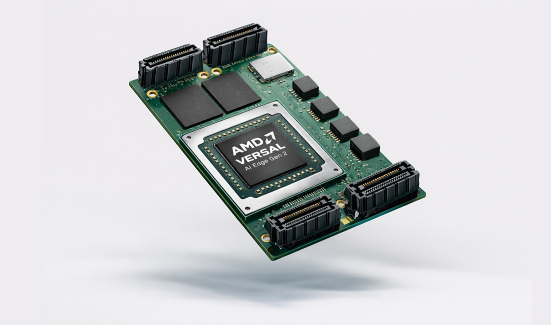
A new generation of the FMC specification has been introduced and is adapting to new technology driven by serial connected devices. Key players in the FMC industry have already begun adopting this specification. Figure 3 shows the first Xilinx demonstration board featuring FMC+, the KCU114. The FMC standard, through its new incarnation FMC+, is alive and kicking and is prepared for the next generation of high-performance, FPGA-driven applications.
Curtiss-Wright www.curtisswright.com
Xilinx www.xilinx.com


