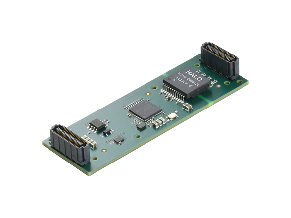
VPX systems are becoming widely deployed in many platforms using high-performance critical embedded computing systems. The flexibility in VPX system conformance is one of the primary factors driving this success. However, the same flexibility creates challenges for system designers using VPX. The abundance of options means that during the development stages, designers would like the ability to test various configurations to determine the best solution for a particular deployment. For low unit volume platforms, configurability is even more important, and the development configuration often ends up as the deployed system.
VPX (VITA 46) backplanes commonly implement high-speed signal standards such as Ethernet, PCI Express (PCIe), RapidIO, SATA, and SAS. It is important to know that when VPX backplanes use these types of signal paths they require point-to-point connectivity from slot to slot to maintain signal integrity and communication speed.
Connecting multiple plug-in cards, such as CPU processor boards, graphics cards, GPU math processors, and the like via a VPX backplane can be problematic because the nature of the extremely high-frequency signals used means that simple “busing” between multiple card slots no longer works effectively.
High-performance, mission-critical backplanes need more flexibility to meet the wide variations in point-to-point signal connection standards. Fabric mapping modules present an effective solution with the necessary signal integrity improvements to meet these challenges, and their use allows many application problems to be solved in the design phase.
From VME to VPX
VMEbus systems (the predecessors of VPX) could accommodate parallel data buses. VITA members eventually developed new standards to accommodate switched serial fabrics that use differential signaling at multigigabit speeds. This necessitated a new connector technology. The differential signaling in switched serial fabrics uses pairs of pins that are physically very close to one another and shielded from other signals by ground pins.
The MULTIGIG RT2 from TE Connectivity was developed to meet the design requirements of VITA 46, now known as VPX. Among its most important features are its quad-redundancy in pin connectivity and the potential for electrical customization. Wafers can be manufactured for differential or single-ended signal paths, and impedance, propagation delay, and cross-talk specifications can be altered per customer requirements.
Consider some examples of backplanes that are built to accommodate the VPX connector:
1. A 3U VPX board with two 16-column, 7-row connectors and one 8-column, 7-row connector.
2. A 6U VPX board with six 16-column 7-row connectors and one 8-column, 7-row connector.
VPX boards have alignment keys that also supply a safety grounding contact. The 6U board has three such keys; the 3U has two (Figure 1).
The density of the VPX connector is such that on a 6U board, there are 464 signaling contacts, which can be allocated as follows:
- 384 differential pins that can be implemented as 192 high-speed differential pairs for core fabric.
- 40 single-ended pins for customer I/O.
- 28 for system utilities.
Even with the impressive performance and capabilities of the VPX connector, the impedance variations imposed by it can create challenges when using the standard overlay techniques of circuit board design. PCB boards that support high-speed signal standards such as PCIe, RapidIO, SATA, SAS, and 10 GbE do so by providing point-to-point direct signaling paths to maintain signal integrity. Consequently, multiple plug-in cards on a backplane cannot share a signal path because communication is no longer done via busing between card slots; the differential-pair nature of the connectors keeps that from being an option.
VPX point-to-point signal standards
The technology of differential-pair transmission is simply the linking of the signal from one transceiver output pair directly to the input of the receiving transceiver by way of two traces that make a 100 ohm transmission line. The VPX connector is made up of small blades, which are actually PC boards in themselves, and continue the 100 ohm transmission line path. The connector’s contacts are a leaf-spring type, which is designed in such a way that any stubs or short lengths of the traces are as short as possible to minimize any signal reflection noise (Figure 2).
Any stub that is present on a signal path will at some frequency cause an additional signal wave front that is out of phase, thus causing destructive interference with the original signal transmission. This interference will diminish the signal seen by the receiving transceiver. The design goal is to optimize the path between the transceivers by eliminating stubs and impedance discontinuities. These factors are further enhanced by a serial protocol that implements pre-emphasis and equalization to make the signal transmission as optimal as possible.
Another aspect of VPX backplane design that one must consider is the adjacencies of the plug-in cards that go into the backplane itself. The closer the source and destination VPX cards are to each other, the faster communication links can be between them. That design aspect, along with the difficulties associated with balanced-pair transmission line implementation, explain why VPX backplanes need more flexibility to meet the wide variations in point-to-point signal connection standards. Micro-overlays – small PCBs for signal routing that are external to the backplane itself – can present an effective solution with the necessary signal integrity improvements to meet this challenge of linking the two requirements.
Using signal mapping micro-overlays
Micro-overlays use ball grid array (BGA) solder connection technology to interface a PCB-based differential pair matrix with compatible backplanes. This reduces transmission line impedance variations and stubs associated with connector-based interfaces by employing the following techniques:
1. Stacked dielectric with alternating etched copper layers implementing signal shield plane and controlled impedance copper etched signal lines.
2. Sub-picosecond matched signal path length. The thickness of the dielectric stack-up is tuned for optimal impedance matching to the signal standard requirements. Off-signal path stub lengths are minimized by this overlay connection technique.
These techniques improve the signal integrity between system cards beyond the requirements of PCIe, RapidIO, and Ethernet standards. Additionally, micro-overlays can also facilitate rear transition modules and low-profile connector interface systems when normal rear transition modules do not fit the system application from a mechanical standpoint (see Figure 3).
Fabric Mapping Modules for VPX backplanes
Dawn VME Products’ Fabric Mapping Modules (FMMs) are micro-overlays that provide benefits to designers of systems using VPX backplanes. Use of FMMs allows the backplanes to be semi-customized and quickly reconfigured according to user needs.
Consider a backplane with power and other utility planes that serve multiple plug-in boards. Those planes need not change or be redesigned when a VPX-based backplane is used for an iteration in the design because FMMs can make iteration-specific changes. Use of FMMs allows for a building-block approach to backplane design, as fundamental, housekeeping planes remain the same, while board-to-board fabric changes can be accommodated simply by changing FMMs. In this way, use of FMMs adds flexibility in system design (Figure 4).
One example is a primary defense contractor that needed help with a four-slot backplane to fit inside a cube-shaped form factor that must be conduction-cooled to fit into multiple vehicle types. Every time the payload plug-in cards are different, but every time the power supply plane is the same. The contractor used processor cards and graphics cards from different manufacturers. The changes in plug-in cards have not forced the design team to completely redesign the backplane because they use FMMs to accommodate the necessary changes on the backplane that correspond to the differences in plug-in cards and front I/O pin-out.
Another example in the use of FMMs is for a major supplier of deployable radio systems based on the VPX backplane. This company’s system makes use of processor cards, storage cards, switch cards, and radio cards that go into different plug-in slots in the backplane depending upon the specific configuration the company needs. They rely on different FMMs to make the configuration-specific connections.
Additionally, this major supplier implements connectors on the FMMs themselves to pick off signals such as Ethernet, SATA, and RS-232, and then routes those signals directly to the system’s front panel. None of these changes requires backplane redesigns because of the inherent flexibility granted by the FMMs.
Use of FMMs in high-performance, mission-critical VPX backplanes (Figure 5) gives system designers the flexibility they need to meet the wide variations in point-to-point signal connection requirements and allows many application problems to be solved in the design phase.
Dawn VME Products www.dawnvme.com


