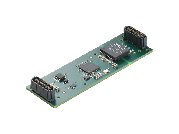
The FMC technical community has been working diligently on upgrades for what is known as FMC+, calling for a new set of connectors to support higher-speed serial interfaces. FMC+ augments the FMC interface by adding 14 additional full duplex high speed serial lanes for 24 total. Beyond FMC+, VITA 57.4 also has a provision for even more high-speed serial lanes. FMC+e calls for a mechanically separate connector to the primary FMC+ connector, adding eight more high-speed serial lanes, bringing the total possible to 32.
The engineering community has been getting creative in ways to leverage the modularity of FMC. Let’s take a look as some of those applications.
Optimizing pin utilization with FMC stacking
By Abaco Systems
Advances in I/O technology have led to multiple signal types being defined for the FMC interface. Additionally, FPGA density and complexity has led to higher device cost, making I/O pins a valuable commodity in any FPGA-based system. Rapid advancement in both FPGA and ADC/DAC technology has led designers to favor modular solutions to accommodate future upgrades without requiring a complete system re-architecture.
The FMC connector is a 400-pin interface accommodating both low-voltage differential signaling (LVDS) and high-speed serial pins as shown in Figure 1. It should be noted that the term ‘serial lane’ often refers to a bundle of two differential pairs: a mezzanine-to-carrier (M2C) differential pair and a carrier-to-mezzanine (C2M) differential pair. This distinction is critical to understand the FMC stacking technology. It is important to note that I/O and clocks dedicated to serial lanes often require connection to specialized pins on the FPGA. Thus, engineers must take care when designing both carrier and FMC to ensure these pins are mapped appropriately.
FMC interfaces are designed to accommodate both LVDS and high-speed serial interfaces. Often, FMC designs don’t require using all I/O, leaving valuable FPGA pins unused and wasted. If intentionally designed in, these unused pins can be utilized by passing these wires to the topside of the board in an intelligent way to enable FMC stacking.
An example of a board with this capability is the Abaco Systems FMC216 shown in Figure 2. This design includes 16 analog output channels at 312.5 MSPS at 16-bits. The FMC216 requires eight high-speed serial lanes from the carrier-to-mezzanine (C2M) and four of the LVDS lanes. This leaves the FMC216 with 10 M2C lanes, 2 C2M lanes, and 76 LVDS lanes unused.
VITA 57.1 calls for all LVDS and serial lanes to be populated in ascending order; thus, the FMC216 re-maps unused pins from the bottom of the board to the top of the board starting at index zero on its respective bus. The topside FMC interface now only has 76 LVDS I/O, all 10 M2C lanes, and only 2 C2M lanes – making it a partially compliant FMC site. If a subsequent FMC board only requires a subset of the LVDS or high-speed serial lanes, an additional FMC can be stacked. The Abaco Systems FMC116 is designed to specifically pair with the FMC216 to create a compact MIMO solution with 16 DACs and 16 ADCs. This matched pair can then be placed on any compliant carrier board.
Limitation and practical considerations
FMC stacking is a way to utilize more of the valuable resources on the FMC interface and connect more sensing capabilities to a single FPGA card, thus reducing the overall system cost. However, it does require the pair of FMCs to be analyzed carefully to ensure compatibility. FMC stacking is a natural consequence of the evolution of I/O types and the FMC standard accommodating both LVDS and high-speed serial. When utilizing FMC stacking, engineers must account for the additional spacing required – often calling for an additional slot in PCIe or VPX systems. Special cooling considerations may be required depending on the FMC type.
FPGA and I/O technologies have shown significant evolution over the past 25 years, from very simple devices to systems-on-chip (SoC) with 1000s of pins. System integrators are more often looking to build systems on modular components based on standard interface. VITA defined the FPGA mezzanine card to accommodate both parallel and serial I/O pin classes: however, many FMC board designs don’t use all available resource pins, leaving extremely valuable FPGA I/O unused. FMC stacking is a technique to get back unused pins on an FMC interface. The CES821 with the FMC216 and FMC116 was given as an example of an integrated solution implementing this technique to not only use as many of the valuable FPGA pins as possible, but also do so in an extremely compact embedded system. When considering I/O system requirements in an FPGA-based system, it is possible to leverage Abaco FMC Stacking technology to ensure valuable FPGA pins do not sit idle.
PXI, meet FMC
By Sundance Multiprocessor Technology
PXI and FMC have different roots and have historically served differing markets. So separate are the markets, that most users are familiar with either one or the other, but not both. However, creatively combining the two standards onto a single product can expand the advantages of either past their current application space.
PXI is a modular pluggable card-based standard common in test and measurement applications. It was released as a standard in 1997 as an abbreviation for PCI eXtensions for Instrumentation, and is maintained by the PXI Systems Alliance. PXI adopts the rugged CompactPCI form factor and adds integrated clocks, triggers, and synchronization critical to test and measurement applications. PXI modules fit into a multi-slot chassis, and are configured and managed by a PC and software. As PCI speeds increased by the adoption of PCIe (PCI Express), PXI has followed with high-speed PCIe fabrics in the chassis and on the modules. Though occasionally referred to as PXIe, PXI remains a generic name, whether the backplane relies on PCI or PCIe.
PXI and FMC standards can be combined into a single product by creating an FMC-compatible PXI carrier card that allows the insertion of FMC modules. In this case, the user will end up with a fully PXI-compatible module, but with the raw measurement function defined by the FMC. Additional processing can be done by the FPGA on the carrier, on another PXI module, or by the PC software, to customize the measurement functions.
An example of this approach comes from Sundance DSP, with their PXIe700 FPGA PXIe Carrier Module. (See figure 4). The PXIe700 is a 3U PXI Express module with a FMC “site” where an arbitrary FMC module can be inserted. The mechanical positioning of the site aligns the faceplate of the FMC module with the faceplate of the PXI card, making it one integrated PXI device.
The PXIe700 carrier supports PXI control, trigger, and clocks to the backplane, including four-lane Gen 2 PCIe communications. It also supports the HPC (High Pin Count) connector to the FMC, including 10 GTX transceivers at 12.5Gb/s each, as well as 144 single ended I/Os or 72 differential I/Os.
All of this is made possible by the onboard Xilinx Kintex7 FPGA, which connects between the PXI backplane and the FMC HPC connector. This can be seen in the Figure 5 block diagram. FMC, by its very name, is intended to interface directly with the I/O pins of an FPGA. This makes for a very high-performance low-latency interface.
Applications
The combination of a high performance PXI carrier with any of the hundreds of FMC modules allows a wide set of applications to be addressed. Though PXI was conceived as a test and measurement platform, its small rugged form factor has also allowed it to be deployed as an embedded application in industrial, medical, and military markets.
An example is using the PXIe-700 with the FMC-DAQ2P5 mezzanine to address radar applications. The FMC-DAQ2P5 hosts a 12-bit 2.7Gs/s ADC (analog-to-digital converter), two 16-bit 2.8Gs/s DACs (digital-to-analog converters), and a number of single ended and differential I/O lines. This is a good example of the high performance instrumentation that can be hosted on an FMC module. In this case, IP is downloaded into the Xilinx FPGA that both analyzes and generates the high frequency signals used in radar applications. Using Mathworks Simulink, the user can add custom algorithms. These signals may be wideband baseband signals, which can be coupled to microwave downconverters, and upconverters available in the PXI format to address the spectrum of interest. Using PXI plus FMC, a small, powerful radar system can be prototyped in a small PXI chassis.
FMC also fills an important role in PXI systems – customization. In many systems standard PXI modules need to be augmented with custom tailored instrumentation or signal conditioning. FMC allows a user to design their own custom printed circuit board that then is deployed in a PXI system via a carrier card. If more board space is needed than available on a standard FMC module, a custom design can be created that is nearly the size of a PXI module. As long as the custom board places the FMC HPC connector correctly, the new daughter card acts as a supersized FMC. If power dissipation is a concern, the new FMC can extend into the space of an adjacent slot, where the PXI chassis will supply ample cooling.
Sundance was not the first organization to deploy PXI plus FMC. CERN did as well, in a very sophisticated data acquisition and control system. The possible applications are only limited by the measurement functionality of FMC modules, which is growing rapidly. The combination expands PXI’s addressable market from primarily test and measurement to data acquisition and control, embedded, and prototyping applications. It is also an effective method for a user to add their own custom card to a PXI system.
PXI metrology grade instrumentation coupled with the growing number of analog, digital, and RF products from FMC is a powerful combination. PXI has addressed a wide set of applications in numerous industries. Over 1500 modules are available from over 50 vendors. With PXI-based FMC carriers, the new applications are nearly endless.


