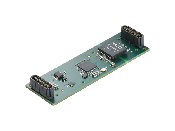
TEWS TECHNOLOGIES increases its I/O offering with the TXMC638, a standard single-width Switched Mezzanine Card (XMC) compatible module providing a user configurable Kintex-7 FPGA with 24 ADC input channels.
Designed for industrial, COTS, and transportation applications, where specialized I/O or long-term availability is required, the TXMC638 provides a number of advantages including a customizable interface for unique applications and a FPGA-based design for long-term product lifecycle management.
The TXMC638 ADC input channels are based on the Linear Dual 16-Bit 5Msps Differential LTC2323-16 ADCs. Each of the 24 channels has 16-bit resolution and works up to 5Msps. The analog input circuit is designed to allow input voltages up to ±2.5 V on each input-pin resulting in a ±5 V differential voltage range.
For customer specific I/O extension or inter-board communication, the TXMC638 provides 64 I/Os on P14 and 4 Multi-Gigabit-Transceiver on P16. The P14 I/O lines are connected directly to the FPGA and can be used as 64 single ended LVCMOS24 or as 32 differential LVDS25 interfaces. Additionally, the TXMC638 provides three 100 Ohm terminated ac-coupled, differential inputs with wide input voltage range.
All front I/O lines such as the ADC interface and the three 100 Ohm inputs are connected to a 98-pin Samtec ERF8-049 Rugged EdgeRate Connector. A 1GB, 32 bit wide DDR3 SDRAM is connected to the user FPGA. The SDRAM-Interface uses an internal Memory Controller of the Kintex-7.
The user FPGA is configured by a serial SPI flash. For full PCIe specification compliance, the XILINX Tandem Configuration Feature can be used for FPGA configuration. XILINX Tandem Methodologies “Tandem PROM” is the favored methodology. The SPI flash device is in-system programmable. An in-circuit debugging option is available via a JTAG header for read back and real-time debugging of the FPGA design (using Xilinx “ChipScope”).
User applications for the TXMC638 with Kintex-7 FPGA can be developed using the design software Vivado Design Suite. A license for the Vivado Design Suite design tool is required.
TEWS offers a well-documented FPGA Board Reference Design. It includes a constraint file with all necessary pin assignments and basic timing constraints. The FPGA Board Reference Design covers the main functionalities of the TXMC638.
The TXMC638 is delivered with the FPGA Board Reference Design. The user FPGA can be programmed via the on-board Board Configuration Controller (BCC). Programming via the JTAG interface using an XILINX USB programmer is also possible. In accordance with the PCI specification and the buffering of PCI header data, the contents of the user FPGA can be changed during operation.
All TEWS products feature a five-year warranty.
About TEWS TECHNOLOGIES
TEWS TECHNOLOGIES is a leading solutions provider of embedded I/O and CPU products based on open architecture standards such as PMC, XMC, IndustryPack® (IP), CompactPCI, standard PCI, PCIe, mPCIe, AMC, FMC, and VME. TEWS has more than 30 years of experience designing and building turn-key embedded interface solutions using the philosophy to listen and respond to our customers’ needs. Using this ‘customer first’ approach, TEWS has developed a large number of standard and custom products for industrial control, telecommunication infrastructure, medical equipment, traffic control and COTS applications. TEWS’ line of embedded I/O solutions is available worldwide through a global network of distributors. For more information, go to www.tews.com.


