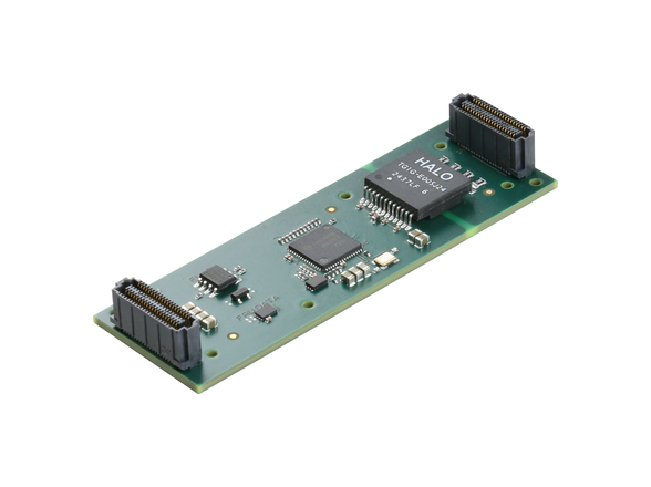
| Altera Corporation’s Stratix® III FPGA family |
AN JOSE, Calif., Nov. 8 — Altera Corporation (Nasdaq: ALTR) today announced its Stratix® III FPGA family, delivering the industry’s lowest power consumption of any high-density, high-performance programmable logic device. Built on TSMC’s 65-nm process, Stratix III FPGAs feature groundbreaking innovations including hardware architecture advancements and Quartus® II software enhancements. Working together, these new features deliver 50 percent lower power, 25 percent higher performance and 2x the density compared to previous generation Stratix II devices.
Altera® Stratix III FPGAs feature two new technologies that dramatically lower power while meeting high-performance requirements. Reduced power consumption is achieved by utilizing Altera’s innovative Programmable Power Technology, which maximizes performance where needed while delivering the lowest power elsewhere in the design. Programmable Power Technology enables every programmable logic array block (LAB), DSP block and memory block to independently operate at high-speed or low-power mode. The PowerPlay feature in Quartus II software version 6.1 automatically analyzes the design and identifies which blocks are in the critical path and demand the highest performance, setting these to high-speed mode. All other logic is automatically put into low-power mode. The second power-optimizing feature, Selectable Core Voltage, provides the designer options to select either 1.1V for designs needing the highest performance or 0.9V for designs requiring minimum power consumption.
“The OneBase family of Base Station Systems offers network operators a range of techniques and deployment technologies to meet build-out requirements and deliver coverage, capacity and high-quality service to end-users,” said Bob Suffern, vice president, research and development at Andrew Corporation. “The Stratix and HardCopy families have been a key enabler of Andrew’s success in this space. And Stratix III, with its lower power consumption, higher integration and path to HardCopy III structured ASICs remains at the heart of our design plans.”
Stratix III devices offer the highest memory-to-logic ratio and DSP performance compared to any other FPGAs in the industry. To address a full range of high-end applications, three new Stratix III family variants are offered: one delivering balanced logic, memory and DSP resources for general-purpose applications, a second providing enhanced memory and DSP resources for memory- and DSP-intensive applications and a third offering integrated transceivers for high-bandwidth interface applications. Additionally, Altera provides a unique and risk-free migration path from Stratix III FPGAs to HardCopy® structured ASICs.
“As high-end FPGAs are increasingly used as the heart of many electronics systems, it is critical for OEMs to achieve new levels of performance and density while minimizing power consumption,” said Jordan Plofsky, Altera’s senior vice president of marketing. “Stratix III FPGAs feature a perfect combination of hardware enhancements and new software capabilities designed to maximize productivity. Our customers can now design their next-generation systems with confidence and successfully get to market quickly and efficiently.”
Stratix III Features
The Stratix III family architecture is based on the same FPGA fabric as the industry-leading Stratix II family featuring high-performance adaptive logic modules (ALMs). Working together, Stratix III FPGAs and Quartus II software offer the industry’s most innovative design methodology for improved productivity and performance. This enables designers to efficiently move their designs from development to production and meet both technical and business goals. Stratix III features include:
— Programmable Power Technology: Enables every programmable logic array
block (LAB), DSP block and memory block to independently operate at
high-speed or low-power mode. The PowerPlay feature in Quartus II
software automatically controls the mode of each block based on
performance requirements.
— Selectable Core Voltage: Enables designers to choose 1.1 V core voltage
for high-performance applications or 0.9 V core voltage for the lowest
power consumption.
— Highest Performance: Stratix III devices are 25 percent faster than the
prior generation and, at a minimum, provide a full speed grade
advantage over any competing FPGA family.
— Highest Density: Stratix III FPGAs bring a 2x density advantage over
prior generation FPGAs and are the highest-density FPGAs in the
industry.
— Flexible I/O: Supporting over 40 I/O interface standards, Stratix III
I/Os deliver industry-leading performance, flexibility and signal
integrity.
— External memory interfaces: Industry-leading memory interface
performance with programmable I/O delay, programmable drive strength
and slew rate, read/write leveling and 31 embedded registers per I/O
for maximum DDR3 performance are new to Stratix III FPGAs.
— Superior signal integrity: Stratix III FPGAs utilize increased
power/ground to user I/O ratio, optimized signal return paths,
adjustable slew rate control, staggered output delays and calibrated
on-chip termination for best-in-class signal integrity.
— Highest-performance DSP capability: Stratix III FPGAs deliver up to
300 times more multiplier/accumulator performance than the
highest-performance digital signal processors, while providing lower
power, smaller board footprint and lower overall system costs for
equivalent performance.
— TriMatrix memory: Stratix III TriMatrix memory includes three sizes of
memory blocks, MLAB blocks, M9K blocks and M144K blocks, that enable
higher memory bandwidth than any other FPGA memory architecture and up
to 17 Mbits of memory performing at 600 MHz.
— Design security: Stratix III devices are the only FPGAs with support
for 256-bit Advanced Encryption Standard (AES) volatile and non-
volatile security key to protect designs from copying, reverse
engineering and tampering. This feature brings ease-of-use and
industry-leading IP protection.
— Quartus II PowerPlay software: PowerPlay optimization and analysis
technology automatically analyzes designs and optimizes them for the
lowest power while meeting users design constraints. No other power
optimization software is as easy to use or effective in minimizing
power.
— Quartus II software v6.1 advanced design features: Quartus II software
version 6.1 enables the highest levels of productivity and the fastest
path to design completion for high-density FPGA designs with the
TimeQuest timing analyzer, top-down and bottom-up incremental
compilation and multiprocessor support. See
www.altera.com/QII6.1release for further information.
Third-Party Support for Stratix III FPGAs
In addition to the Quartus II design software, tools from leading EDA vendors Aldec, Inc. (System Verification Environment (SVE)), Magma Design Automation Inc. (Blast FPGA), Mentor Graphics® Corporation (Precision® Synthesis) and Synplicity, Inc. (Synplify Pro FPGA synthesis and Synplify DSP software) all support the Stratix III device family, ensuring the highest quality of results in Altera devices.
Availability and Pricing
Engineering samples of the first member of the Stratix III device family will be available in the third quarter of 2007. Customers can start their Stratix III designs today using Altera’s Quartus II design software version 6.1. 1000-unit pricing starts at $549 for the EP3SL150 device in 2007. For more information about Stratix III devices, visit www.altera.com/stratix3 .
About Altera
Altera’s programmable solutions enable system and semiconductor companies to rapidly and cost-effectively innovate, differentiate and win in their markets. Find out more at www.altera.com .


