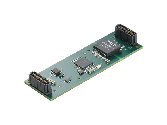
HILLSBORO, OR – November 28, 2011 – Lattice Semiconductor Corporation (NASDAQ: LSCC) today redefined the low cost, low power mid-range FPGA market with its announcement of the next generation LatticeECP4™ FPGA family, with 6 Gbps SERDES in low cost wire-bond packages, powerful DSP Blocks and hard IP-based Communication Engines for cost- and power-sensitive wireless, wireline, video, and computing markets. The LatticeECP4 FPGA family builds on the award winning LatticeECP3™ family by bringing premium features to mainstream customers while maintaining industry-leading low power and low cost. The LatticeECP4 devices are ideal for developing mainstream platforms for a variety of applications such as Remote Wireless Radio Heads, Distributed Antenna Systems, Cellular Basestations, Ethernet Aggregation, Switching, Routing, Industrial Networking, Video Signal Processing, Video Transmission and Data Center Computing.
A video demonstration of the LatticeECP4 FPGA Family can be viewed here:
English: www.latticesemi.com/ecp4videoen
Chinese: www.latticesemi.com/ecp4videocn
Japanese: www.latticesemi.com/ecp4videojp
Images of the LatticeECP4 FPGA Family can be viewed and downloaded here: www.latticesemi.com/ecp4images
High Quality SERDES and Hardened Communication Engines
The LatticeECP4 FPGAs contain up to sixteen CEI-compliant 6 Gbps SERDES channels with embedded Physical Coding Sub-layer (PCS) blocks in both low cost wire-bonded and high performance flip chip packages, giving customers the choice to deploy the LatticeECP4 FPGA in chip to chip as well as long haul backplane applications. The versatile and configurable SERDES/PCS can be seamlessly integrated with the hardened Communication Engines to economically build complete high bandwidth sub-systems. The Communication Engines offer up to 10X the power and cost reduction of similar implementations in FPGA fabrics. The LatticeECP4 Communication Engines portfolio includes solutions for PCI Express 2.1, multiple 10 Gigabit Ethernet MAC and Tri-speed Ethernet MACs as well as Serial Rapid I/O (SRIO) 2.1. The combination of SERDES/PCS and Communication Engines is ideal for completing complex serial protocol-based designs with lower cost, power and footprint while accelerating time to market.
Innovative DSP Processing Reduces Multiplier Count
The LatticeECP4 family features powerful digital signal processing (DSP) blocks with 18×18 multipliers, wide ALUs, adder-trees and carry chains for cascadability. Unique booster logic means each LatticeECP4 DSP block can be equal to four LatticeECP3 DSP blocks, enabling up to 4X the signal processing capability of the previous generation LatticeECP3 devices. The flexible 18×18 multipliers can be split into 9×9 or combined into 36×36 to perfectly match customers’ application requirements. Moreover, up to 576 multipliers can be cascaded together to build complex filters for wireless Remote Radio Heads (RRH), MIMO-based RF antenna solutions and video processing applications.
Higher Performance and Capacity
The LatticeECP4 FPGAs are up to 50% faster than previous generation devices and feature 1066 Mbps DDR3 memory interfaces and 1.25 Gbps LVDS I/Os that are also capable of being provisioned as serial Gigabit Ethernet interfaces. The new LatticeECP4family also has 66% more logic resources and 42% more embedded memory to empower design engineers to construct complete systems-on-chip in FPGAs.
“The next generation LatticeECP4 FPGA family offers our customers an unprecedented combination of the premium features, high performance, low cost and low power that is necessary for sophisticated but cost sensitive wireless, wireline, video and computing applications. Lattice has been a pioneer in providing cutting-edge innovations in economical devices for our customers. With the LatticeECP4 devices now included in our Lattice Diamond® design software, our customers can begin immediately to build broad-based, lower power platforms to expand their markets,” said Sean Riley, Lattice Corporate Vice President and General Manager, Business Group.
Design Support for LatticeECP4 FPGAs
Lattice provides intellectual property (IP) cores, development boards and design software for quick launch of design initiatives and rapid time to market. A range of intellectual property (IP) cores will include CPRI, OBSAI, Serial RapidIO, XAUI, SGMII/Gigabit Ethernet, PCI Express, SMPTE for serial connectivity, FIR filters, FFT, Reed-Solomon encoders/decoders, CORDIC, CIC, NCO for DSP functions and several others for memory interfaces and connectivity.
Lattice Diamond Design Environment Accelerates Development Time
Customers can begin designing with LatticeECP4 FPGAs now using the Lattice Diamond 1.4 beta design software. Lattice Diamond design software is the new flagship design environment for Lattice FPGA products and provides a complete set of powerful tools, efficient design flows and a user interface that enables designers to more quickly target low power, cost sensitive FPGA applications. In addition, Lattice Diamond software continues to provide industry-leading features specifically developed for low cost and low power applications. These include a very accurate power calculator, pin-based simultaneous switching output noise calculator and proven MAP and PAR FPGA implementation algorithms that help ensure low cost and low power design solutions. To learn more about the Lattice Diamond Design Environment, please visit: www.latticesemi.com/latticediamond.
About the LatticeECP4 FPGA Family
The LatticeECP4 FPGA family is comprised of six devices that offer standards-compliant multi-protocol 6G SERDES in low cost wire-bond packages, DDR1/2/3 memory interfaces with speeds up to 1066 Mbps, and powerful, cascadable DSP blocks that are ideal for high performance RF, baseband and image signal processing. Toggling at 1.25 Gbps, the LatticeECP4 FPGAs also feature fast LVDS I/O as well as embedded memory of up to 10.6 Mbits. Logic density varies from 30K LUTs to 250K LUTs with up to 512 user I/O. The LatticeECP4 FPGA family’s high performance features include:
• DSP blocks that allow up to 36×36 Multiply and Accumulate functions running at >500MHz. The DSP slices also feature innovative cascadability for implementing wide ALU and adder tree functions without the performance bottlenecks of FPGA logic. The DSP block offers booster logic, which allows 4X the bandwidth per DSP block relative to previous generation DSP architectures.
• 6 Gbps SERDES CEI-6G jitter compliance and the ability to mix and match multiple protocols on each SERDES quad. This includes PCI Express 2.1, CPRI, OBSAI, XAUI, Serial RapidIO 2.0, SGMII/Gigabit Ethernet and 10 Gigabit Ethernet.
• The SERDES/PCS blocks have been designed specifically to enable the design of the low latency variation CPRI links that are found in wireless basestations with Remote Radio Head connectivity.
• Hardened Communication Engine blocks using hardened metal arrays featuring multiple 10GbE and Triple Speed MAC blocks, as well as PCI Express 2.1 and SRIO 2.1 blocks. These blocks are 10X more area- and power- efficient that traditional FPGA-based implementations.
• Compliance to the SMPTE Serial Digital Interface standard, with the unprecedented ability to support 3G, HD and SD video broadcast signals independently on each SERDES channel. The triple rate support is performed without any oversampling technique, consuming the least possible amount of power.
• 1.25 Gbps LVDS I/O, with Clock Data Recovery blocks, allows interfacing to high performance ADCs/DACs and implementation of SGMII/GbE links. The ability to perform CDR functionality on general purpose I/O greatly increases the number of serial I/O available to the designer, allowing smaller FPGAs to be used even when a large number of SERDES channels are needed, greatly reducing the cost of implementing serial Ethernet interface logic.
These features make the LatticeECP4 FPGA family ideally suited for deployment in high volume cost- and power-sensitive wireless infrastructure, wireline access equipment, video and imaging, as well as computing applications. For more information about the new LatticeECP4 FPGA family, please visit www.latticesemi.com/ecp4.
Availability
Select customers are already designing with LatticeECP4 FPGAs using the Lattice Diamond 1.4 beta design software. Device samples will be available in the first half of 2012 and high-volume production delivery is scheduled for the second half of 2012.
About Lattice Semiconductor
Lattice is the source for innovative FPGA, PLD, and programmable Power Management solutions. For more information, visit www.latticesemi.com.


