Embedded and industrial system architectures are typically based on a modular approach. The venerable VME, then CompactPCI followed by CompactPCI Express, the AMC form factor, and even the emerging VPX (VITA 46) form factor all represent different implementations of the “modular-board-plugged-onto-a-backplane” concept. The market for industrial computers will probably remain focused on the plugged-onto-a-backplane technology for years to come. And other electronic systems designers, such as those developing military embedded systems, are also willing to take advantage of the flexibility and field upgradeability of the modular concept offering.
This is now the case for FPGA boards, too, with the unlimited flexibility levels of FPGAs restricted only by the physical interfaces around the programmable logic device. Hence, the interface buffers, transceivers, or any kind of physical interface between the FPGA’s I/O and the outside world dictate the interface protocol the FPGA will host, independent of the final application. If all FPGA applications had homogenous characteristics, this would lead to a plethora of boards looking very similar (in shape, FPGA-surrounding resources, and backplane interfaces), except for the physical connection.
This is a very ironic and almost criminal scenario, since the FPGA is the most versatile electronic device available today. This variety is exemplified in terms of the FPGA’s internal features and general-purpose logic blocks, of course, in addition to PLL, memory, and hardware IP. External features are also subject to wide adaptability, with different voltage, single-ended as well as differential, and high throughput.
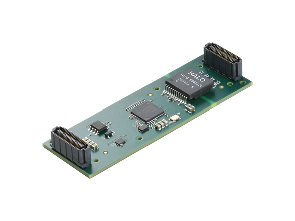
The FPGA Mezzanine Card, standardized as VITA 57 and known by its acronym, FMC, brings a convenient answer to the need of I/O flexibility when using FPGAs. The following discussion focuses on FMC’s emergence from other mezzanines, presents an in-depth look at FMC melded with AMC, and examines the ironic constraints imposed by FMC’s ultimate flexibility.
FMC emerges from other mezzanine standards
The practice of moving onto a mezzanine the I/O features likely to change from one application to another also applies to both CPU expansion mezzanines and to FMCs. There is, however, a major difference: Connecting a CPU core to an expansion mezzanine implies the need for communications protocols to establish connection with the I/O mezzanine. PMC mezzanines use the PCI bus, and this idea later evolved into the XMC form factor with a connection through PCI Express. (Figure 1 depicts a typical SBC architecture with a CPU core and PMC/XMC expansion.) PCI was also used for the PC-MIP; meanwhile, older mezzanine formats used processor buses (IP-Modules, M-Modules).
Regarding CPUs, rackable architectures can be seen as I/O expansion devices for a central CPU board. Such systems use parallel buses such as VME and CompactPCI, as well as serial interconnect systems such as PCI Express, GbE, and Serial RapidIO. Parallel buses use single-ended lines, and fast serial links use differential signaling; thus, the market tends to focus on standards, increasing bandwidth and reducing pin counts.
The technical aspects are very different for FPGA/FMC I/O interfaces, however, as compared to I/O for a CPU. (Figure 2 depicts an architecture with an FPGA and FMC mezzanine site.) For FPGAs, an I/O management mezzanine board needs to have connections as undefined as possible; this leaves FPGA designers with a choice as to the types of I/O technology to implement. The more numerous and versatile FPGA signals that exist, the better, whether single-ended or differential. FMC makes this ultimate I/O flexibility possible, while standardizing and defining some aspects of the design to provide increased modularity, while still leaving some choices up to designers.
FMC: Under the microscope
Anyone assigned to write a specification has been confronted with the burden of imagining what future users will require, while trying not to leave out important assets.
Some applications will require a lot of single-ended signals, with varied voltage levels. Others will need low-throughput differential pairs. And high-performance applications will demand high-throughput differential pairs, this time with imposed directions. The FMC concept brings flexibility to these and other paradigms, with its:
- 34 differential pairs or 68 single-ended signals on the basic Low-Pin-Count (LPC) connector version
- An additional 24+22 differential pairs or 48+44 single-ended signals on the extended High-Pin-Count (HPC) connector version
- One carrier-to-mezzanine differential clock and one mezzanine-to-carrier clock on the LPC connector
- One carrier-to-mezzanine differential clock and one mezzanine-to-carrier clock on the HPC connector
- 10 differential high-speed carrier-to-mezzanine signals, 10 differential high-speed mezzanine-to-carrier signals, and 2 differential clocks from mezzanine to carrier
- Management signals such as geographical addressing, Power-Good indicators, and a Mezzanine Presence detector
In addition to stand-alone FPGA-plus-FMC applications, the FMC concept can also be utilized with standard embedded computing form factors including 6U/3U CompactPCI, VME, or VPX, as well as AMC boards.
A complete case is depicted in Figure 3, which shows an Altera ARRIA-II GX FPGA-based AMC board. The FPGA is the central operating device. Hence, high-speed communication channels are used for backplane communication and for high-speed devices on the FMC module, for whichever implementation it might be, for example, fiber-optic communication or 10 GbE. Again, the FMC provides improved I/O flexibility.
Low-cost applications can also take advantage of a Low-Pin-Count FMC. Apart from clocks and management signals, the FMC connector offers 34 general-purpose differential pairs that can also be used as 68 single-ended signals. For example, a Low-Pin-Count FMC module with four MIL-STD-1553 channels uses four National Hybrid NHI15LV65_CSP44 transceivers, each one consuming 12 FMC I/O interfaces for a total of 48. The FMC offers sufficient real estate for four transceivers and the eight line transformers. Keep in mind that FMC does not intend to provide complete interface functions as other mezzanine formats such as PMC and XMC do; rather, FMC intends to move the physical interface devices and circuitry to a mezzanine, thus bringing flexibility to FPGA carrier boards.
PCB design considerations
The PCB is of primary importance when considering FMC. The FMC utilizes a surface-soldering connector type, which the PCB designer will call Ball Grid Array (BGA), even if the connector itself does not contain solder balls. The pitch is 1.27 mm, allowing the PCB to be manufactured in class 5 with 0.25 mm via finished hole dimensions. With the LPC connector version where the contacts are arranged as two sets of two 40-ball rows, it is even possible to route the signals in class 4. This FMC versatility shows a real concern for cost control, especially on the mezzanine side. On the carrier side, the PCB class and routing technology are dictated by the FPGA and its associated resources. A ball pitch of 1 mm is common and leads to track thickness smaller than what is required for the FMC carrier connector.
Blessing or curse: FMC flexibility yields constraints
VITA 57’s description of communication signals between the FPGA and the FMC states clearly that both operating voltages and signal direction are FMC-dependant. Additionally, the FMC mezzanine must carry an identifying EEPROM that allows the carrier board to determine which FMC is actually mounted, to match FMC I/O signaling to the FPGAs. This flexibility, as part of the FMC concept, is fundamental but can also lead to a number of constraints – and choices – for the FPGA designer:
1. The FPGA configuration file depends on the FMC; the FPGA must be loaded with the appropriate file, once the FMC is known. If the FPGA is in charge of examining the FMC to which it is connected, then the FPGA will be powered up with a configuration file that disables all I/O between the FPGA and the FMC but allows the FPGA to access the data in the ID EEPROM. The FPGA is to then reload itself with the appropriate file so it can start working with the proper FMC.
2. The process of identifying the FMC may be left to a persistent programmed device: a CPLD or a microcontroller. In this scenario, the FPGA is externally loaded with the appropriate content. However, a precaution shall be made for EEPROM-based FPGAs: The device must have a global I/O disabling signal to isolate the FMC and the FPGA when the CPLD/CPU gets the FMC information and, if needed, reprogram the FPGA.
3. FPGAs are loaded with a global configuration file. This means that the carrier board must have, stored somewhere, one configuration file for each FMC the board is likely to receive. If the FPGA has more than one FMC, the number of configuration files rises exponentially. To place several FMCs on a carrier board, it is more efficient to use mid-range FPGAs, one per FMC, and to design an inter-FPGA communication process. This internal bus may also be used in conjunction with a local CPU or CPU module, as well as a PCI-to-local bus bridge.
FMC spawns burgeoning ecosystem
The FMC concept will spawn a wide range of products and services: FMC modules with multiple and heterogeneous communication standards; FMC carriers with or without CPUs; complete systems bringing together CPU-on-Modules and FPGA-plus-FMC blocks. The reason it matters: The FMC concept spreads the I/O modularity concept to FPGA applications. Split a design using modules, and engineering expenses will be cut in half.
Nolam Embedded Systems +33 1 73 71 30 06 www.nolam.com


