The greatest challenge facing developers of embedded systems is the diversity of external I/O interfacing requirements. Whether it be Ethernet, optical, analog conversion, or gigabit serial, system developers need the facility to efficiently construct the necessary mix of interfaces. Over the past two decades, the FPGA has proven itself to be the ideal component to directly interface with I/O transceivers since it can adapt to the demands of protocol and bandwidth needs.
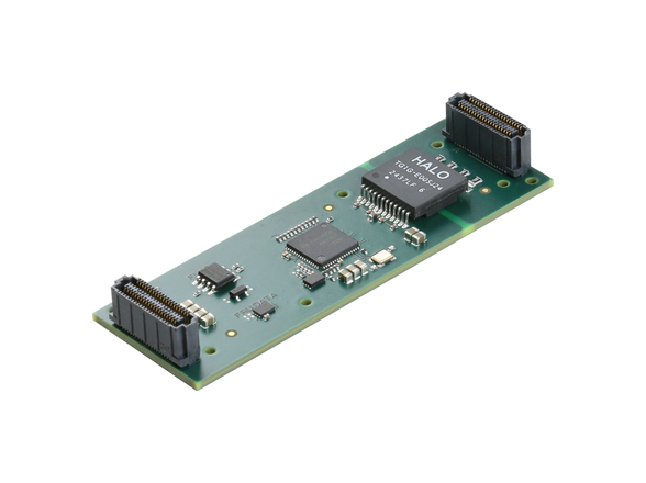
System designers have successfully used mezzanine modules such as PMCs and XMCs, which enable carrier cards to be personalized with the required I/O interfaces. Building on the mezzanine I/O concept and embracing the reconfigurable nature of FPGAs, the VITA 57 FPGA Mezzanine Card (FMC) standard is the first open standard I/O mezzanine module for FPGAs.
The FMC architecture decouples the I/O interfaces on the mezzanine module from the FPGAs located on the carrier card. This strategy greatly simplifies the design of the I/O interfacing modules, which now only require the core I/O transceiver circuitry. For example, consider an I/O module that requires two ADC channels. Using an FMC, the design of the mezzanine module only requires front-end analog conditioning and two ADC converters, together with the supporting power supplies. With an XMC implementation, an additional protocol device (for PCI and/or Serial RapidIO) is required with the interfaces for the protocol implemented. This is then linked to the ADC converters, typically using an FPGA. Apart from adding material and labor costs, power consumption is typically increased by 2 W. On the other hand, the size of the FMC mezzanine is approximately half that of an XMC while retaining comparable area for I/O circuitry.
Situating the FPGAs on the carrier card drives this simplification of the mezzanine module design and equally important, it maximizes carrier card reuse. With the increased capacity of FPGA and I/O pins, carrier cards can be designed such that they can be repurposed to a range of application areas. Furthermore, as new generations of FPGAs are released, carrier cards can be upgraded and utilize the library of FMC modules already developed.
By leveraging the capabilities of FPGAs, FMC brings a range of benefits including:
- Maximum data throughput – Individual signaling speeds up to 10 Gbps, with a potential overall bandwidth of 40 GBps between mezzanine and carrier card.
- Minimal latency – Complete elimination of protocol overhead removes latency and also ensures determinism of data delivery.
- Reduced design complexity – I/O is connected directly to the FPGA, hence expertise in protocol standards such as PCI, PCI Express, or Serial RapidIO is not required.
- Minimal system costs – Simplifying the system design reduces costs for IP cores, engineering time, and materials for the finished product.
The versatility of FMC data handling is equally complemented by a range of environmental configurations that span low-cost commercial-grade through to ruggedized conduction-cooled options.
FMC has been gaining a lot of traction during its development. Following its ANSI approval in July 2008, the interest has continued to accelerate. A variety of solutions from mechanical components to high-performance FPGA compute carrier cards is already available, and further significant announcements will be made in the coming months.
Malachy Devlin of Nallatech is the FMC/VITA 57 chairperson. For more information on VITA 57, email Malachy at [email protected].
Reference – VITA Standards Activity Chart (July meeting highlights)

