Fiber optics are commonly deployed in telecommunications and data center applications where bundles of fibers are used for communication links. Optical fiber cable can be used as a medium for telecommunication and computer networking because it is flexible and can be bundled as cables. It is especially advantageous for long-distance communications, because light propagates through the fiber with little attenuation compared to electrical cables. This allows long distances to be spanned with few repeaters. Telecommunications led the charge with fiber optics for long-haul transmission lines and wide area networks (WANs). Datacom followed, using fiber optics for local area networks (LANs) within data centers in rack-to-rack and intra-rack networks. Figure 1 illustrates how fiber optics have migrated from telecom to the computing industry within the past 15 years.
High-performance system overview
The demand for higher bandwidth throughout the entire architecture of a computer network is continuously pushing the need for speed. Processor performance has far outstripped I/O performance and is craving faster pipes to get data to and from the processing engines. The growth in demand has been greatest in systems, which are I/O intensive rather than computing intensive. A typical system requires the routing of data from many inputs to many outputs, as is found in switched serial fabric architectures such as VPX.
The mesh topologies of the VPX switched serial fabric-based architectures create complex levels of interconnection, which is especially significant when compared to the previous VME parallel bus architecture.
The level of fault tolerance and scalability offered by these topologies is also significant; however, this forces increased complexity and cost into the backplane, particularly when platforms support protocols with bit rates up to 5.0 Gbps. A fully populated VPX blade supports 192 pairs and 48 single-ended signals.
In terms of PCB design and manufacture, the challenge of developing a backplane with 192 differential pairs in a mesh architecture is significant and costly. Copper traces must be impedance controlled, which means that they must be referenced to a ground plane. Consequently, for each high-speed routing layer there also must be a reference plane, as well as layers for power and slow-speed signals. Therefore, it would not be too difficult to conceive that backplanes in the future with 30 to 40 layers will be necessary to build systems with Terabit routing requirements.
In order for these type of platforms to scale further than 10 Gbps, the level of interconnect will have to rise proportionately or the link speed will have to increase. If a full mesh topology requires 40 Gbps between blades, then this will require more than 5,800 copper traces on the backplane in a bidirectional 14 node system and more than 800 connections per blade.
Challenges of copper technology
The first obvious solution to this problem would be to increase the point-to-point link speed over copper traces. However, there are fundamental problems with pushing the serial link speed of copper above 5 Gbps through a typical backplane configuration. Additional environmental effects such as temperature and humidity compound the problems facing designers, as well as manufacturing variation in the PCBs and connectors. This forces backplane designers to use more expensive techniques and materials.
Substrates other than FR-4 carry a premium, and the same goes for microvias, buried vias, and backdrilling to eliminate via stubs, along with increasingly more complex and expensive backplane connectors. Even with transceivers that incorporate pre-emphasis in their drive circuits, the effects of insertion loss, crosstalk, and jitter can degrade signals such that operation above 5 Gbps is not viable.
Optical backplane requirements
There is a clear advantage to increasing serial link speed as opposed to increasing the number of interconnects. The most prominent option would be to use optical interconnects; however, this presents a number of issues in itself. The adoption of optical interconnects for use in VPX and other switched fabric environments would have to meet the following demands:
- Optical must coexist with copper on a substrate in order to draw power and slow speed management interfaces.
- Connectors must be pluggable for field-replaceable units (FRUs).
- Optical connectors must operate under current environmental conditions in the chassis.
- The backplane must be a passive electrical and optical element of the system.
- The solution must be cost-effective.
Optical interconnect challenges
The first demand of optical interconnection concerns the development of a mixed copper and optical PCB where both can coexist. Several companies offer fabrication of optical PCBs incorporating high-density parallel multimode polymer waveguides. The methods used for manufacturing such PCBs and the tolerances involved are compliant with current techniques, which when combined with a set of design rules, allows waveguides to be laid out by PCB designers in the same fashion as copper.
Waveguides can either be formed on the surface layer of a PCB or embedded within internal layers of the FR-4. Several polymers are available today with characteristics suitable for backplane applications, such as resilience to high temperatures needed for solder processes, low loss at conventional optical wavelengths, and good immunity to long-term degradation.
The second issue concerns the requirement that optical connectors need to be pluggable in a similar fashion to copper connectors. The main problem with optical interconnects concerns the alignment of the driver and receiver elements to the waveguide. Parallel waveguide structures are typically in the order of 70 μm cross-section on a 250 μm pitch, so it is critical to have a reliable, low-cost, and repeatable method of connector alignment. Furthermore, 90-degree corners and multidrop requirements add to the complexity of a pluggable backplane design.
The third point is that it would be mandatory that any optical connector must be able to operate within the parameters of temperature, vibration, and reliability required for platforms that currently use copper interconnects. System availability of 99.999 percent remains a key requirement in telecom and datacom markets; however, in the military markets this is often extended even further.
Point four highlights the fact that existing copper backplanes are passive elements, thus any optical backplane should also be a passive element. Blade systems are popular in applications where they can be removed, especially when a system shutdown is not required. Any fault in an active backplane system would require a complete strip down in order to replace it, something which is not considered acceptable. The implementation of backplane interconnects should not use active switch components in either copper or optical systems.
The final and perhaps most important point is that in order to be cost-effective, an optical solution should be able to match the price point of copper interconnect or offer a performance improvement metric. Although many different cost models are available for copper vs. optical, the real inflection point will likely be driven by other market conditions such as competition or technology innovation in markets outside of the telecom, datacom, or computercom markets. Cost will remain an excuse until someone else does it first. The industry might have to create and accept new cost models that take into consideration the bandwidth performance of blades and systems in order to break through the cost barrier.
To prevent unnecessary conversions from electrons to photons and back, the complete pipeline must be optical. Today, there are too many conversions in a typical system. Optical implementations will really gain traction when the complete chip-board-backplane-board-chip data path can be implemented over optical waveguides.
New form factors for boards, blades, and backplanes might need to be considered. Designers have stuck with the typical four-sided, multilayer PCB, but what if they tried using other geometries and 3D or 4D dimensions? Would a new pluggable optical backplane be better suited if it were a cylindrical or other shape? New concepts for servers are already emerging from Facebook’s Open Compute Project (www.opencompute.org) that could displace traditional motherboard and blade architects.
Competing technologies that are under research now are also slowing down commercial adoption. There is still ongoing debate between free-space and waveguide transmission, and even within each of these options, there are derivatives supported by competing suppliers. It is going to take a large player in the market making a stand to make one option or another bubble to the top. Waveguide technology seems to have the upper hand, but the technology is still in its infancy.
Optical waveguide technology also holds the promise of enabling passive optical splitters that are independent of data rates, which means that electrical point-to-point buses could potentially be replaced by optical multidrop buses. The possibility of in-plane waveguide crossings could enable a reduction of board layer count. In addition, optical waveguide technology is unaffected by electromagnetic interference, which might be an important factor in hostile or sensitive environments.
Current industry status
Optical innovation lags in board-to-board (backplane) and chip-to-chip implementations. Many papers have been written and demonstrations made of possible solutions, from waveguide backplanes to embedded optical fibers in a backplane. Several years ago, Defense Advanced Research Projects Agency (DARPA) saw the need for research on chip-to-chip optical interconnection and provided funding for studies on Terabus from 2009 to 2011. Unfortunately, this program is no longer funded by DARPA. IBM produced several demonstrations of Terabus (see Figure 2), but it has never progressed beyond the research stage.
The February issue of the Journal of Lightwave Technology published a white paper titled “Pluggable Electro-Optical Circuit Board Interconnect Based on Embedded Graded-Index Planar Glass Waveguides” that goes into great depth on electro-optical circuit boards (ECOBs) that could possibly be used as the foundation for future optical backplanes. Waveguides offer several advantages over fiber that make their use in backplanes attractive.
I attended the Optical Fiber Communication Conference and Exposition (OFC) in Los Angeles last March. I was hoping to learn more about research on backplanes with optical fibers or waveguides. All I found were a couple of outdated (10-plus-years-old) demonstrations in the IEEE booth. Both demonstrations highlighted connector technology for tapping off the back of a backplane to link into a run of fiber-optic cable. No signs of functional optical backplanes were in sight.
The Optical Internetworking Forum (OIF) conducts an annual interoperability testing. The tests conducted in August 2014 included three demonstrations on backplane connector technology that were a bit more up-to-date. These demonstrations showed the OIF-28G-VSR interface comprising a Xilinx evaluation board, a length of cable, and a Finisar CFP4 evaluation board exhibiting interoperability across both electrical and optical interfaces at 25+ Gbps.[1] Again, no practical optical backplane implementations were demonstrated.
More recently, a panel of industry experts met at DesignCon 2015 to discuss the topic “Will the Optical Backplane Ever Happen?” Rick Merritt, UBM, EETimes, captured these comments from the panelists:
- The optical backplane of the future is still a far future dream. Optics are superior to copper in reach, enabling a larger chassis, but “optics have not demonstrated power efficiency – you waste all the energy in optoelectronic conversions,” said Hong Liu, a Principal Engineer in Google’s platform group.
- “The feasibility of cost-effective manufacturing is highly unlikely in the short term,” said J. Balachandran, a senior Cisco Systems engineer. Dense wavelength-division multiplexing (WDM) will open a door to 100x greater I/O density in systems, a capability that eventually will make a move to optical backplanes inevitable. “That will change the system architecture radically, but there are still a lot of factors to solve, and cost is a key one,” he added.
- Ed Priest, a Distinguished Engineer at Juniper Networks, predicted a switch to optical backplanes could come at 200G data rates, two major generations from now. “What’s finally going to tip it is …[at some point the SERDES] won’t fit on the ASIC anymore, and once [that happens] you can design a new custom I/O chip that opens [the system] up to optics,” Priest said. “I’m pretty convinced at 100G [serial rates the electronics] will work, but at 200G I don’t know yet,” he said.
- “I predict the percent of optical backplanes will continue to grow, but very slowly,” said John Monson, VP of sales at SERDES designer MoSys. “They won’t become predominant until electrical alternatives fail, and that won’t happen anytime soon,” he said.
These experts are from the telecom and datacom industries, so their comments must be taken from that perspective. The computercom industry has not been able to fully leverage optical connectivity, and thus is under a different set of pressure points to make decisions perhaps a bit sooner.
VITA member initiatives
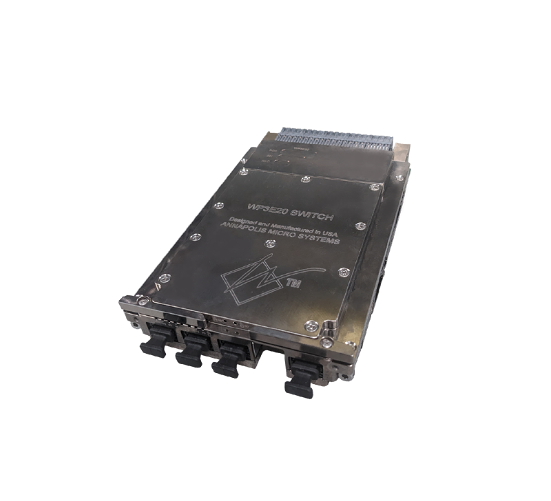
VITA members have been working on an early generation of optical interconnection with the work done in VITA 66. Blind-mate optical connectors are implemented in a pass-through fashion, allowing backplanes and plug-in modules to mate with the ability to then pass the optical link on to a fiber cable that can be routed either internally or externally to a system. This is still not a fully pluggable optical backplane, but it is solving the problems for now. VITA members Elma Electronics and Pentek have announced products that implement the VITA 66 standard (see Figures 3 and 4).
VITA architectures for optical study group
VITA members recognize the need for higher-density, higher-performing interconnect technologies to meet the speeds of 10 Gb and higher serial channels that will be used in next-generation critical embedded systems.
Achieving the projected level of combined performance and connector density is no easy challenge. The lead time to develop technologies and supporting specifications is very long. To that end, VITA launched a study group, VITA Architectures for Optical Study Group, with the mission to research and determine the feasibility of developing a standard architecture for optical interconnects suitable for deployment in critical embedded systems. The study group is focused on high-density options for backplanes and connections between line-replaceable units, mezzanines, and daughtercards.
The study group will move to working group status as the need to develop specifications emerges. Existing standards and those under development by standards developing organizations (SDOs), as well as appropriate industry alliances, community collaboration efforts, and other groups will be used whenever practical. The study group will proactively reach out to such groups to facilitate their early involvement. Interested parties are invited to participate in the study group discussions. For more information, visit www.vita.com/VAO.
Innovation on the horizon
Optical interconnects must overcome considerable challenges before they can become a reliable technology in critical embedded computing systems. However, the combination of high-speed, low-power, small-footprint, optoelectronic modules with a data rate-scalable transmission medium promises to meet the demands of future ultra-broadband onboard and backplane interconnection.
While no serious advancements have been made in the development of practical and deployable products using optical interconnections at the board or chip levels, the technology is slowly advancing, leaving room for more innovation. Optical backplanes are still on the horizon, but we are getting closer.
References
[1] Multi-Vendor Interoperability Testing of CFP4, QSFP28, and Backplanes with CEI-28G-VSR and CEI-25G-LR Interface During ECOC 2014 Exhibition (September 2014) www.oiforum.com/public/documents/OIF_Interoperability_ECOC2014_White_Paper_Final.pdf


