Data acquisition and control is an important aspect of most systems such as manufacturing, control, research, or anything that accepts data and controls. Adding FPGAs to data acquisition provides pre- and post-algorithmic processing on data. In choosing how to construct the system, a number of items must be considered. The hardware elements chosen should have features that make the modules easy to program and handle, while the FPGAs should be reprogrammable when required. These requirements, along with module density and sophistication, cost, and availability with the latest A/D and D/As, formed the basis for our own search for a suitable data acquisition system.
Our company, Joerger Enterprises, chose VME as the fundamental module type because of the wide availability of interoperable and reliable boards and the standard’s longevity. VME was designed in the 1980s, but the VITA standards body has constantly updated it to provide the latest features. These upgrades were always downward compatible so that older modules remained usable. Its latest pure bus-based version, VME64x, is both VME- and VXI-compatible. (The latter is ideal for test and measurement.) VME also offers some EMI/RFI noise protection – a definite requirement in high-frequency data acquisition applications. However, VME wasn’t our only choice for the modules. We also considered standards based upon PCI, VXS (VITA 41), VPX (VITA 46), GbE (VITA 31.1), and even PC-based “computer motherboard” modules.
Why VME?
The features that VME offers are extensive. From the original 32-bit bus, the connectors P1 and P2 have been increased from 96 to 160 pins. This added additional ground pins, +3.3 V power pins, a provision for two higher voltages for special applications, and additional leading-edge +5 V and ground for theoretical live insertion and extraction. There’s also a geographical address implementation and provisions for additional future pins. Data read/write on the leading and trailing clock edges through the 2eSST protocol greatly improves access and throughput on the bus. Also, +3.3 V power pins and additional ground pins provide the ability to use PWB power and ground planes for better layouts. This latter is a critical feature because the switching speed at which FPGAs operate must be well filtered (see Sidebar 1).
Although access speed on VME has improved for data acquisition systems, it can still be a problem since large DRAMs can store tremendous amounts of data. To facilitate a faster I/O pipe, VITA has added a third rear connector called P0 mounted between P1 and P2. Besides user-defined I/O, high-speed pipes such as PCI Express, Serial RapidIO, GbE, or InfiniBand can interface on P0.
But P0 serves another important use in data acquisition systems: access to mezzanine (“daughter”) card resources. Due to VME’s large ecosystem of COTS modules, Joerger Enterprises discovered several popular VME series with mother/daughtercards featuring ADCs, DACs, registers, logic, motor controllers, and timing and control signals that could be run to the backplane via P0. However, we were unable to source a VME card set to handle the type of sophisticated applications our customers require. Despite our best efforts to use off-the-shelf, it was decided we needed to design our own VME card set.
Designing new modules: Basecard
Designing new modules is difficult and time-consuming, not the least of which is complicated by the rapid improvements in ICs. Physical chip sizes keep getting smaller, speeds increase, and density is greater – all factors that make new designs go obsolete quickly. For example, ADCs are now available with two channels; speeds are in excess of 125 MHz at 14-bit resolution, they consume much lower power, and they’re available in a 9 mm square package. On the output side, DACs are available with clock speeds greater than 500 MHz at 14-bit resolution, and they boast excellent glitch-free operation in a tiny 7 x 10 mm package. Clock generators with an internal PLL and VCO capability can produce 500 fsec jitter-free clocks in a 9 mm package. In addition, many ADCs and DACs are now available using serial techniques. These are valuable as converters or offset and gain controls for more sophisticated chips.
As far as our own VME card set, using a well-designed motherboard would allow the module to be designed with daughtercards: a much quicker, less-expensive solution. Our motherboard interfaces with the VMEbus. An FPGA interfaces to the VMEbus, the front panel, and daughtercards. We decided that the motherboard would accept four daughtercards, each with its own FPGA and two SRAM memory chips. Another motherboard option accepts up to four daughtercards without the arrays and memory. This layout is for less-complex modules with the master FPGA controlling the daughtercards. A full motherboard is shown in Figure 1.
To provide control, a number of on-card buses are provided: one that routes to all the local SRAM arrays, individual buses to each daughtercard FPGA/memory array, and individual clocks and I/O to each array. In this way, the master array has complete control. Rear access is available to the motherboard for analog or digital signals from the rear P2 connector. In many instances, rear access provides a cleaner system and avoids many of the problems with inadvertent front-panel connector access.
It’s important to note that not all system requirements call for a card set like ours. There are a number of manufacturers that have mother/daughtercard combinations that should be considered. For modern, high-performance data acquisition systems, FPGAs should be used for logic. They are fast, can perform a large variety of functions, and offer that all-important feature in system design: they’re reprogrammable.
Mezzanine daughtercards
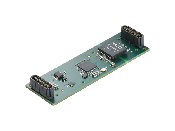
Our daughtercards are independent, and each contains the programming chip for its motherboard array. This chip is available to the JTAG connector so complete programming and reprogramming are possible. The daughtercard interface to the motherboard is important, and two high-speed, 80-pin connectors with a ground bus are provided. Many data acquisition operations require various functions like ADCs, DACs, digitizers, or registers, and having each function on a different daughtercard but operating as one VME module improves density and lowers cost.
Figure 2 shows a daughtercard featuring a four-channel digitizer. The motherboard uses high-speed SRAMs so that read/write data is not compromised. If large memory capacity were required, then DRAMs would be placed on the daughtercards – trading off some performance for sheer memory densities. Each memory is addressed and controlled individually via the array, allowing a great amount of freedom of use. Each memory is 32 bits and 2 Mwords.
Using four of these daughtercards offers 16 individual, 125 MHz, 14-bit digitizers in one VME module – a density not possible with a standard VME board. With four daughtercards installed, this 16-channel digitizer occupies a mere single 0.8" VME slot. CS
Joerger Enterprises, Inc. 631-239-5579 www.joergerinc.com

