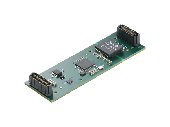
With increasing frequency, FPGAs are showing up in the I/O portion or "front end" of embedded system designs to implement complex I/O interfaces, execute in-stream data processing, and even run user algorithms. FPGAs have naturally migrated to the front end of systems because they are so well suited to I/O and data stream processing; they have a large number of I/O pins, they have built-in support for a variety of I/O standards, and they have large amounts of logic that can be configured to implement protocols and process data. Because of the flexibility and reconfigurability of an FPGA, a single-FPGA design can be reused for a wide range of I/O by reconfiguring the FPGA and changing the I/O interface components such as the physical connectors or transceivers and any required I/O controller chips. However, this still requires a board redesign and respin. With the growing popularity of FPGAs in embedded designs, the embedded community could benefit from an industry standard method of modular I/O for FPGA designs.
For years, the PMC, and more recently the XMC, have provided an industry standard mechanism for a modular and flexible I/O design, primarily for use with 3U and 6U SBCs. The PMC/XMC form factors have been used extensively in the embedded computing realm, but they aren’t the optimal solution for modular FPGA designs. PMCs are much larger than an FPGA I/O mezzanine needs to be, they have the wrong type of and too many connectors, and the interface between the PMC/XMC and the baseboard (PCI, PCI-X, PCIe, Serial RapidIO, and so on) is much more complex and resource intensive than is required for an FPGA I/O mezzanine to interface to an FPGA.
Analogous to how PMCs provide modular I/O for SBCs, there is now an industry standard approach to providing modular I/O for FPGA designs – the FPGA Mezzanine Card (FMC). The FMC (also known as VITA 57) standard was developed to provide an industry standard mezzanine form factor in support of a flexible, modular I/O interface to an FPGA located on a baseboard or carrier card. It allows the physical I/O interface to be decoupled from the FPGA design while maintaining a close coupling between a physical I/O interface and an FPGA. This approach separates FPGA board designs into two pieces – a carrier and a mezzanine. The carrier contains one or more FPGAs and the associated functionality that will always be common to any variation of the board design. The mezzanine contains the functionality that can be variable within a board design, such as the I/O portion of the design.
The FMC approach solves the problem of how to change the I/O configuration of an FPGA design without having to redesign the core FPGA functionality. The FMC brings to FPGA designs the benefits of PMC modules that embedded developers have come to rely on. These benefits include shorter design cycles, increased ease in taking advantage of technology advances, and lower development and recurring costs. An overview of the standard follows.
FMC standard overview
The FMC standard defines an I/O mezzanine module that works intimately with an FPGA. The standard defines two widths – single and double width. Figure 1 illustrates that the single-width module, which measures 69 x 76.5 mm, is approximately half the size of a PMC module, and supports a single connector, P1, to the carrier. The double-width module measures 139 x 76.5 mm and can support one or two connectors to the carrier, P1 and P2. The double-width FMC is for applications that require additional bandwidth to the carrier, more front panel space, or a larger PCB area. As is the case with most commercial PMC/XMC modules, most commercial FMCs will be single width.
There is a choice of two different connectors to interface the FMC to an FPGA on a carrier: a Low Pin Count (LPC) connector with 160 pins and a High Pin Count (HPC) connector with 400 pins. An FMC with the LPC connector can mate with a carrier that utilizes either an LPC or HPC connector. To support the widest range of FMCs, commercial carriers should utilize the HPC connector. The FMC specification was developed to enable FMCs to be supported on a wide range of existing form factors including but not limited to VME, CompactPCI, VXS, VPX, VPX-REDI, CompactPCI Express, AdvancedTCA, and AMC. Figure 2 shows three FMCs fitted to a 6U VPX carrier.
The VITA 57 connector was chosen to ensure developers have the functionality and performance they need to allow them to move their I/O to a mezzanine card. The connector is designed to support single-ended and differential signaling up to 2 Gbps and signaling to an FPGA’s Multi-Gigabit Transceivers (MGTs) up to 10 Gbps. The LPC connector provides 68 single-ended user-defined signals or 34 user-defined differential pairs, one MGT pair, clocks, a JTAG interface, and an I2C interface to optionally support the base IPMI commands. The HPC provides 160 single-ended user-defined signals or 80 user-defined differential pairs, 10 MGT pairs, and additional clocks.
To meet the demands of high-performance embedded computing, the FMC connector can support very high bandwidths; a single differential pair can provide 2 Gbps of bandwidth when clocked at 1 GHz since data can be transferred between the FMC and the carrier on the rising and falling edges of the clock. Even when clocked at a conservative 250 MHz, 32 differential pairs provide 2 GBps of bandwidth (250 MHz x 2 clock edges x 32 bits/8 bits/bytes). As an example, a quad 215 MSps 12-bit ADC FMC would transfer data at a rate of 1.29 GBps (215 x 12 bits/ADC x 4 ADCs/8 bits/byte). Utilizing 48 differential pairs (12 bits/ADC x 4) of the HPC connector clocked at 107.5 MHz (one half of the ADC sampling rate) would provide the required bandwidth to move the data from the four ADCs into the FPGA on the carrier.
The MGT interfaces are most useful for supporting protocols that run over multi-gigabit serial links. Moving the copper connectors or fiber optic transceivers from the base-FPGA design to an FMC mezzanine card makes it much easier for a single FPGA design to support various physical interfaces. Next-generation ADC and DAC chips that support the JEDEC JESD204 standard (Serial Interface for Data Converters) interface will directly connect to one or more FPGA MGT ports. Converter chips supporting JESD204 interfaces, such as the Linear Technology LTC 2274 16-bit 105 MSps ADC, are expected to hit the market in 2008.
The FMC standard defines both air- and conduction-cooled form factors. The conduction-cooled form factor can receive all I/O over the P1 connector, or it can support front-panel I/O if necessary. Also defined in the standard is a front-panel bezel, clearly visible in Figure 3, which is very similar to PMC front-panel bezels.
The FMC standard provides for a great deal of flexibility in the interface between the FMC and carrier to support a wide range of functionality FMCs may provide. Flexibility in standards typically equates to incompatibility and fragmentation of the market, but this is not the case with the FMC standard. Even though there can be a wide variability in the number of I/O pins from FMC to FMC, due to the reconfigurability of FPGAs, as long as an FPGA has sufficient I/O pins mapped to the FMC site connector to support a particular FMC, the FPGA can be configured to support that FMC.
FMC benefits
Not surprisingly, an FPGA-based design utilizing an FMC has the same benefits as industry standard mezzanine cards that have been around for years, such as PMC modules, or the newer form factors such as XMCs. The same benefits of utilizing mezzanine cards in CPU-based computing are now available for FPGA-based designs.
One major benefit of VITA 57 is shorter development cycles for design variations. It is intuitive to see that it will be much simpler to change to a new I/O interface if the design utilizes an FMC approach. If an FPGA design needs to support a second I/O interface, the savings will not be profound; the real savings come when a single FPGA design can be utilized in multiple applications or programs by simply developing a new FMC.
Another benefit that mezzanines have provided for years is an improved ability to take advantage of technological advances. If there are advances in I/O, a new FMC module can interface to an existing FPGA carrier. Likewise, when next-generation FPGAs become available, existing FMC modules can be interfaced to the new FPGA carrier to take advantage of the latest in FPGA technology.
One other important benefit is cost. Being able to reuse either FMCs or FPGA carriers, whether using in-house developed boards or COTS designs, will reduce both development costs and recurring costs through the use of fewer and common components across multiple programs. As is the case with PMC modules, the real cost savings will come when developers can purchase off-the-shelf FMCs or FPGA carriers and not have to develop their own boards.
Looking back provides a glimpse into the future
The benefits of PMC modules didn’t come about overnight. It wasn’t until there was critical mass of commercial SBCs with PMC sites and commercial PMC modules that the embedded community was able to realize the inherent benefits. By now, the PMC approach has been taken for granted by developers, and these benefits are expected. The same will happen with FMCs – it will be expected that future FPGA designs will be based on the FMC approach.
Whether designing a proprietary (in-house design) embedded system, purchasing COTS products to integrate, or using a combination of in-house and COTS products, if the design includes FPGAs, the FMC standard can and will make the system designer’s job easier. The standard has gone to the ANSI balloting process but as with many other draft standards, vendors are already developing products around it. There have been no announcements yet, but we should start seeing commercial FMC mezzanines and carriers hit the market in the first half of 2008. CS
Dave Barker is the vice president of market development for embedded solutions at VMETRO. Before joining VMETRO in 2005, Dave was the marketing manager for VME products at the Motorola Computer Group and has worked in the industry for more than 25 years. Dave has a BS in Computer Science from the University of Pittsburgh and an MBA from the University of Phoenix. He can be reached at [email protected].
VMETRO, Inc.
281-584-0728
http://www.vmetro.com


