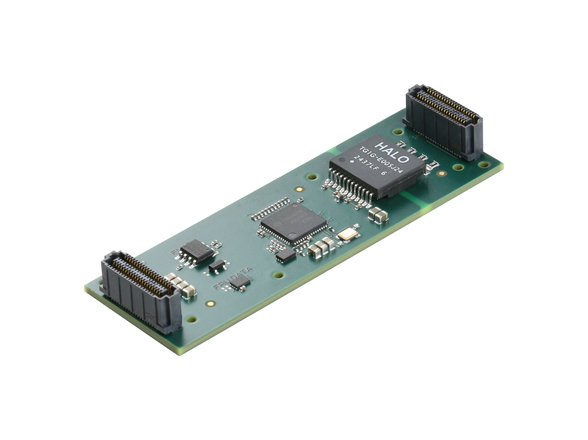
March 22, 2007 – TEK Microsystems, Inc. of Chelmsford MA today announced its new modular VXS architecture. The new approach combines the use of a common, FPGA based digital processing baseboard with a wide range of analog input and output mezzanine modules. This architecture allows system designers to adopt this technology with the assurance that future technology upgrades in either the digital baseboard or analog mezzanine can be made easily and cost effectively, protecting their investment in application firmware and software.
The Janus VXS, also announced today as the first VXS product to combine FPGA based DSP processing technology with seven channels of 16-bit, 500 MSPS DAC (digital to analog conversion) is the implementation of this new modular architecture.
“The new baseboard / mezzanine modular design for our A/D and D/A products provides a highly flexible implementation that enables low risk, efficient insertion of technology upgrades. For our customers, that means the highest performance solutions using the latest technology that fit in smaller spaces,” comments Andy Reddig, president and CTO at TEK Microsystems, Inc. “This architecture provides faster time to market for Tekmicro and easy migration to our next generation of Virtex 5-based products.”
A New Modular Architecture
Janus VXS is the first implementation of TEK Microsystems’ new baseboard / mezzanine modular architecture developed for its 6U VXS products. The baseboard currently uses the Virtex II Pro FPGA. The next generation of baseboards will include Virtex 5 FPGAs and is expected to be available in the fall of this year. Customers purchasing products today can easily upgrade to the new platforms with minimal changes to their application firmware or software.
By placing the FPGA processing functionality on a base card and keeping the D/A and A/D interfaces on a mezzanine card, the resulting implementation provides several key benefits:
– Faster time to market. By reusing a standard back end FPGA processing baseboard for multiple products, Tekmicro can more quickly respond to customer and market needs.
– Improved signal integrity and fidelity. Careful definition of the mezzanine interface and component layout ensure the highest possible analog performance.
– Improved range of front end analog options. Within this architecture, Tekmicro will offer the broadest available range of analog bandwidths and resolutions from 100 MHz to 3 GHz.
– Easy technology insertion. For Tekmicro and for customers, as either analog or FPGA processing technology advances, the products can be easily upgraded, protecting the customer’s investment in firmware and system development for the long term.
– Common firmware and software development architecture – Whichever hardware product you are using, customers will benefit from extensive reuse of hardware and firmware components across the full range of interfaces and form factors, minimizing learning curves and development cycles.
About TEK Microsystems, Inc.
Founded in 1981 and headquartered in Chelmsford, Massachusetts, TEK Microsystems, Inc., designs, manufactures and markets a wide range of advanced high-performance boards and systems for embedded real-time data acquisition, data conversion, storage and recording. The Company provides both commercial and rugged grade products which are used in real-time systems designed for applications such as reconnaissance, electronic warfare, signals intelligence, mine detection, medical imaging, radar, sonar, semiconductor inspection and seismic research. For additional information see www.tekmicro.com.

